|
STELLA NEWS SITE is managed by Stella Corporation Inc. |

| ORIGINAL ARTICLE | CD-ROM (English virsion) | |||
|
üĪExhibition Reportü@ |
Original CD-ROMs 2025 edition (Device Manufacturing Process) have been
released at May, 2025
|
|||
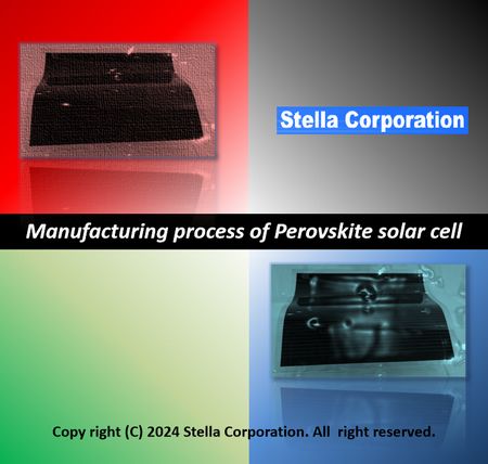
nanotech 2026 Mass-Production Coater System for Perovskite Solar Cells Supporting 1,200 mm Width Unveiled 40th NEPCON JAPAN Active Proposals for New Processes for Perovskite Solar Cells |
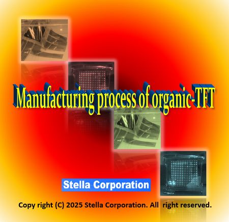
Manufacturing process of organic-TFT |
|||
|
üĪConference Reportü@ |
||||
| üĪHEAD LINE NEWS | ||||||||||||
|
üĪKaneka Begins Outdoor Demonstration Project of Tandem Perovskite Solar
Cells with Saitama City |
||||||||||||
| üĪEVENT Schedule in Japan | ||||||||||||
|
| STELLA NEWS SITE is a free news site of FPD and PCB by Stella Corporation Inc.(This company does not release these FPD and PCB related products.) Stella Corporation Inc. 1-1544-7 Kaijincho Minami, Funabashi, Chiba, Japan Zip: 273-0024 Tel: +81-(0)47-432-5031 Fax: +81-(0)47-432-5032 E-mailüFinfo@stellacorp.co.jp |