|
|
STELLA NEWS SITE is managed by Stella Corporation Inc. |

|
FPD/PCB NEWS〜November 28
|
|
Sumitomo Chemical Reaches Agreement to Acquire Taiwanese Semiconductor Process Chemicals Company Sumitomo Chemical annouced to enter into a definitive agreement to acquire 100% of the shares of Asia Union Electronic Chemical (“AUECC”), a Taiwanese semiconductor process chemicals company. The transaction is subject to customary closing conditions, including obtaining required regulatory approvals. |
|
FPD/PCB NEWS〜November 25
|
|
|
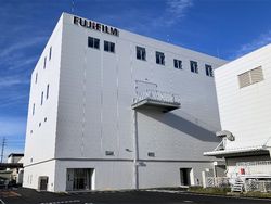
Fujifilm Announces Completion of a New Building for Advanced Semiconductor Materials in Shizuoka
The new building at the Shizuoka Factory is equipped with state-of-the-art evaluation equipment in a high-cleanliness cleanroom, enhancing quality evaluation functions for development and production. AI image recognition technology has been introduced to inspect fine particles contained in semiconductor materials, improving analysis accuracy and establishing an advanced quality control system utilizing AI. Furthermore, a department promoting digital transformation (DX) has been established in the new building to support the expansion of digital technologies such as AI in manufacturing processes, thereby improving product quality and ensuring stable supply. |
|
FPD/PCB NEWS〜November 21
|
|
|
TEL Construction Completed on Tokyo Electron Technology Solutions'Tohoku Production and Logistics Center
The new building is a hybrid logistics center that combines production and warehouse functions. By consolidating logistics warehouses presented in and around the prefecture and improving production efficiency, the center will reduce lead times and solve operational problems in production and logistics, including human resource shortages and the implementation of business continuity planning. This will make the operations more flexible, efficient, and responsive. |

|
FPD/PCB NEWS〜November 17
|
|
EBARA to Establish Second Overhaul Plant for Dry Vacuum Pumps in Korea Ebara Precision Machinery Korea Incorporated (EPMK), a subsidiary of EBARA CORPORATION, is to construct a second overhaul (OH) plant for dry vacuum pumps in Pyeongtaek, Gyeonggi Province, Republic of Korea. This initiative will further enhance EBARA's supply structure and after-sales service capabilities in the Korean market. |
|
FPD/PCB NEWS〜November 12
|
|
|
SATO Develops Printing-Based RFID Antenna Manufacturing Technology Using Conventional Micron-Sized Copper Paste
Compared to conventional methods that use aluminum (Al) or silver (Ag) pastes, the new technology achieves higher conductivity and stable quality suitable for mass production, while also reducing manufacturing costs. The company is exploring applications and mass production possibilities in fields such as circuit fabrication, sensor development, and solar cell substrate wiring formation, and is also considering co-creation with partner companies. |

|
FPD/PCB NEWS〜November 7
|
|
Ritsumeikan University:PFAS Decomposed into Fluoride Ions Using Low-Toxicity Semiconductor Nanomaterials A research team led by Professor Yoichi Kobayashi of the College of Life Sciences at Ritsumeikan University, together with Shuhei Kanao, a master's student in the Graduate School of Life Sciences, has successfully decomposed and detoxified “forever chemicals” known as PFAS (per-and polyfluoroalkyl substances)?which pose environmental and health risks. Specifically, they achieved the breakdown of perfluorooctanoic acid (PFOA), which is internationally regulated, and perfluorooctanesulfonic acid (PFOS), known for its extreme resistance to degradation.The team demonstrated that by combining low-toxicity, inexpensive, and mass-producible zinc oxide (ZnO) semiconductor nanocrystals with a commercially available near-ultraviolet LED light source, PFAS can be decomposed into fluoride ions under ambient temperature and pressure conditions. The resulting fluoride ions can be reused as fluorspar (calcium fluoride), the mineral raw material used in industry. |
|
FPD/PCB NEWS〜November 6
|
|
Nagoya University Researchers Achieve Sub-Nanometer Thickness Control of Amorphous Silica Nanosheets A research group led by Assistant Professor Eisuke Yamamoto and Professor Minoru Nagata at the Institute of Materials and Systems for Sustainability (IMaSS), Nagoya University, has successfully synthesized amorphous silica nanosheets whose thickness can be precisely controlled at the sub-nanometer level, using a solid-phase surfactant templating method.By employing solid-phase surfactants containing polyethylene oxide (PEO) chains as templates, the researchers were able to freely tune the nanosheet thickness through molecular design of the surfactants. The resulting nanosheets exhibited high dispersion stability, and it was confirmed that they could form densely packed two-dimensional films. Further investigation into the influence of nanosheet thickness on their properties revealed that, although the band gap remained constant regardless of thickness, thinner nanosheets showed higher dielectric breakdown strength. |
|
FPD/PCB NEWS〜November 5
|
|
JSR and IBM to Strengthen Semiconductor Materials Development Using AI JSR and IBM have signed a Joint Research Agreement to launch a collaborative research program focused on AI for the chemical industry.Through the expansion of foundation models specialized in materials development and the utilization of generative AI to enhance data infrastructure, the two companies aim to build an integrated platform for managing diverse material systems. They also plan to conduct joint research to establish knowledge frameworks that enable the understanding and modeling of a wide variety of material representations. |
|
FPD/PCB NEWS〜November 4
|
|
SCREEN Acquires Nikon's R&D Business for Wafer Bonding Technology SCREEN Holdings announced to acquire Nikon's research and development business related to wafer bonding technology.SCREEN positions the advanced packaging field as a key strategic area and has been promoting the development and implementation of low-temperature wafer bonding technologies, in addition to marketing direct imaging systems and coater/dryers. Through this acquisition, SCREEN aims to integrate Nikon's ultra-high-precision bonding technologies and expertise with its own existing technologies, pursuing the realization of world-leading wafer bonding capabilities. |
|
FPD/PCB NEWS〜October 31
|
|
BASF to Build Electronic-Grade Ammonium Hydroxide Plant in Ludwigshafen, Germany BASF has announced plans to build a state-of-the-art electronic-grade ammonium hydroxide (NH4OH EG) plant at its Ludwigshafen site in Germany to support wafer cleaning, etching, and other precision processes in semiconductor manufacturing.The NH4OH EG produced at the new facility will be essential for advanced-node chip technologies, enabling the next generation of semiconductors that are crucial for Europe's key industries, including the automotive sector and artificial intelligence. |
|
FPD/PCB NEWS〜October 29
|
|
YKK AP Begins Demonstration of Grid-Connected Interior Windows Using Glass-Type Perovskite Solar Cells for Building-Integrated Photovoltaics YKK AP announced to begin a demonstration project at the “Tanimachi YF Building” in Osaka City, integrating interior windows equipped with glass-type perovskite solar cells into the power grid as part of a Building-Integrated Photovoltaics (BIPV) system.As a step toward commercialization and practical application, the company removed the existing interior windows in the office areas on the 6th and 7th floors of the Tanimachi YF Building and replaced them with new BIPV windows, completing construction and grid connection. |
|
FPD/PCB NEWS〜October 28
|
|
Waseda University and Toin University of Yokohama Develop Upconversion-Type Perovskite Solar Cells Capable of Utilizing Near-Infrared Light A research group led by Associate Professor Ayumi Ishii of Waseda University's Faculty of Science and Engineering and Specially Appointed Professor Tsutomu Miyasaka of Toin University of Yokohama's Faculty of Biomedical Engineering has developed a technology that immobilizes organic dyes?capable of absorbing weak near-infrared light?onto rare-earth-based nanoparticles, converting that light into visible light through upconversion.Furthermore, by incorporating these nanoparticles into perovskite solar cells, the team successfully converted near-infrared light?previously unusable with conventional lead-based perovskite devices?into electricity. |
|
FPD/PCB NEWS〜October 27
|
|
NEDO and JAIST Sign Memorandum of Understanding on Industry-Academia Collaboration The New Energy and Industrial Technology Development Organization (NEDO) and the Japan Advanced Institute of Science and Technology (JAIST) have signed a Memorandum of Understanding (MoU) for mutual cooperation.Under this agreement, both parties will work together to support the matching of researchers with companies and other organizations to promote industry-academia collaboration, as well as to foster human resources for startup support. |
|
FPD/PCB NEWS〜October 23
|
|
Waseda University Develops a Method to Narrow the Search Space for Predicting Organic Molecular Crystal Structures Using Machine Learning A research group led by Associate Professor Takuya Taniguchi of the Data Science Center at Waseda University, together with Ryo Fukazawa, a third-year doctoral student in the Integrated Doctoral Program at the Graduate School of Advanced Science and Engineering, has successfully improved the success rate of predicting organic molecular crystal structures using machine learning.The team developed a crystal structure prediction workflow called SPaDe-CSP, which efficiently narrows down promising candidate crystal structures using machine learning and rapidly optimizes their geometries with a neural network potential. When applied to 20 types of organic crystals, the method successfully predicted crystal structures with a high success rate of 80%, which is twice as high as that achieved by conventional random search methods. |
|
FPD/PCB NEWS〜October 20
|
|
|
Rigaku Establishes Group Company in Taiwan and Launches Full-Scale Operations at New Technology Center
RTC-TW serves as a technology base to promote research and development, customer support, and joint development projects. It features cleanroom facilities that replicate production environments, as well as spaces for demonstrations, training, and collaborative development. The center enables the local team to provide rapid and advanced technical support to customers in the region. |

|
FPD/PCB NEWS〜October 20
|
|
Sekisui Chemical, NTT DATA, and Nikkei Engineering Develop Based on insights and challenges identified through installation demonstrations conducted since 2023 on the exterior wall of the NTT Shinagawa TWINS DATA building, Sekisui Chemical and NTT DATA have developed a mounting method that uses aluminum extruded materials for the fixing hardware. This method aims at practical application by emphasizing light weight and manufacturability. In addition, the partners are examining techniques to easily adjust wrinkles and distortions that tend to occur in film materials during wall installation, while also ensuring aesthetic quality. |
|
FPD/PCB NEWS〜October 14
|
|
Tohoku University, National Institutes of Natural Sciences, and Tokyo University of Science Although the two nanoclusters have nearly identical frameworks, Ag79, which has just one more silver atom in its outer shell than Ag78, exhibits a 77-fold increase in photoluminescence quantum yield at room temperature. The dramatic improvement in luminescence efficiency was revealed, through both experimental and theoretical analyses, to arise from the combined effects of (1) enhanced radiative transitions due to reduced symmetry and (2) suppressed structural fluctuations resulting from changes in the ligand environment. This achievement provides new insight showing that “a difference of just one atom can dramatically alter luminescent properties.” |
|
FPD/PCB NEWS〜October 8
|
|
Fujifilm Launches Advanced Packaging CMP Slurry FUJIFILM announced the launch of CMP slurry for advanced packaging, enabling the integration of multiple semiconductor chips into a single package. This product has been adopted by a major semiconductor device manufacturer as an essential abrasive for planarizing bonding surfaces in hybrid bonding, one of the advanced packaging technologies key to enhancing AI semiconductor performance.The newly launched product is an evolution of Fujifilm's front-end copper interconnect CMP slurry, optimized for advanced packaging. The formulation of additives, corrosion inhibitors, and abrasives has been refined to achieve high-precision planarization of hybrid bonding surfaces, where copper and oxide films coexist. |
|
FPD/PCB NEWS〜October 1
|
|
Tamura and Tohoku University established the “Tamura × Tohoku Univ. Advanced Power Electronics Co-creation Research Center” Tamura Corporation and Tohoku University have jointly established the “Tamura × Tohoku Univ. Advanced Power Electronics Co-creation Research Center” at the University's Material Solution Center (MaSC).The Co-creation Research Center aims to drive research and development of innovative materials, components, devices, and modules that contribute to creating new value in the power electronics market. |