|
STELLA NEWS SITE is managed by Stella Corporation Inc. |

SEMICON JAPAN 2025 (Desember 17 - 19) |
|||||||||
SEMICON Japan 2025 was held at Tokyo Big Sight from December 17 to 19.
Below are selected highlights picked up through a subjective lens.
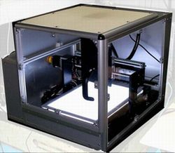
The targets are available not only in circular and rectangular planar types but also in cylindrical rotary types. In recent years, demand for rotary targets offering a high material utilization rate of around 50% has been increasing. Incidentally, in the display field, the targets have already been adopted for mass production by TFT-LCD and OLED manufacturers in China and South Korea, and they appear to be steadily eroding the stronghold long held by conventional IGZO targets. AI-Equipped Systems Improve IJ Printing Stability and Accuracy In manufacturing equipment, Elephantech showcased its presence by exhibiting the actual unit of its high-precision inkjet printer “ELP04 PILOT,” which was specially developed for the company's proprietary nano Cu ink and paste, along with printed Cu ink/paste samples.
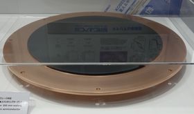
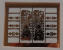
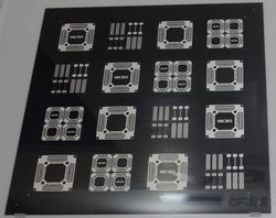
This means that even when printing droplets with a diameter of 20 μm into grooves 40 μm wide, 100% of the droplets land within the grooves. At the booth, samples printed by inkjet on glass and silicon wafers were displayed. Typical printed line-and-space resolution was L&S = 50 μm / 50 μm, demonstrating a 100% yield at this resolution. Fine Patterns Using Ag Sintered Metal for Glass Substrates
Using a commercially available photosensitive Ag paste from Toray (Raybrid) and following coating, exposure, development, and firing processes, the company achieved fine patterns with a minimum L&S of 15 μm / 15 μm. The resulting resistivity was 3 × 10⁻⁶ Ω・cm. However, because the firing temperature is relatively high 500 - 600℃, the process is limited to substrates such as glass and silicon wafers. High-Boiling-Point Solvent Reduces Drying Nonuniformity After Resist Coating In materials-related exhibits, DAICEL introduced a unique high-boiling-point solvent for photoresists called “CELTOL.” With a boiling point of 150 - 200℃, adding 5 - 10 wt% of CELTOL to photoresist allows the film to dry more slowly during the post-coating drying process on the substrate. As a result, coating nonuniformity is less likely to occur compared with photoresists formulated with conventional low-boiling-point solvents. |
|||||||||
| REMARK STELLA NEWS SITE is a free news site of FPD and PCB by Stella Corporation Inc.(This company does not release these FPD and PCB related products.) |
|