FineVision
Simulation Software “Etching Process Simulator” (Optional) |
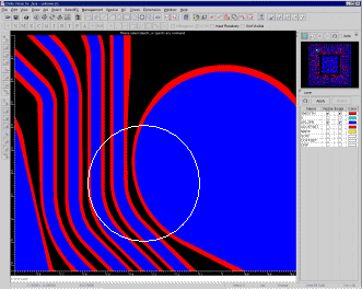
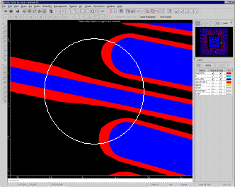
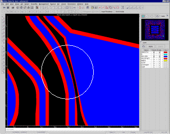
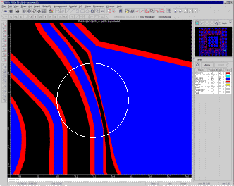
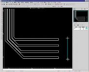
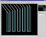
We have succeeded to develop a simulation software “Etching Process Simulator “which is possible to forecast pattern form of photoresist film after exposure and development in advance, as an assisted tool of the exposure process by making use of photomask. This development is realized by adopting of new algorithm on the original CAD/CAM software (Stella Vision) technology. Therefore, we are releasing this etching simulator software as an assisted manufacturing tool for ultra-fine pattern such as a dozen nm (optional). As you know, design rule of semiconductor device is shrunk year by year, however, in the fine design rule from exposure wavelength on down, if a photomask is manufactured by making use of original design data, same exposure pattern such as the original design data is not gained. Therefore, OPC (Optical Proximity Correction) which is calibrated technology of photomask pattern is used in general, to correspond the original design pattern with exposure pattern. In this time, we have developed original simulation software by development of a novel algorithm based on OPC technology. If you make use of this software, you can manufacture an optimized photomask for ultra-fine pattern easily. Figure 1 shows simulation sample image. In this figure, inside purple line is forecast pattern of photoresist after exposure and development, on the other hand, outside sky-blue line is calibration pattern for acquirement of the original pattern. In short, line with becomes to be slightly finer after development by over-development. Of course, calibration level of form is optimized automatically in parallel with placement.
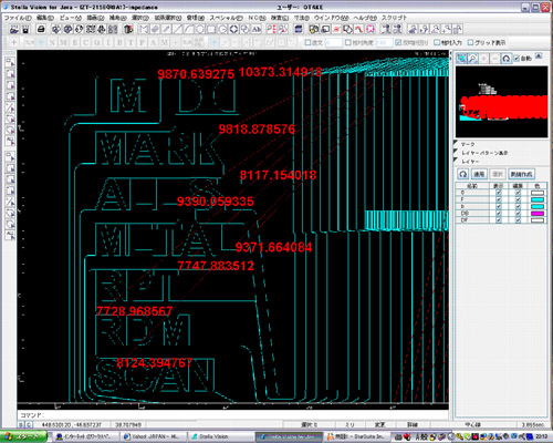
As you know, design rule of semiconductor device is shrunk year by year, however, in the fine design rule from exposure wavelength on down, if a photomask is manufactured by making use of original design data, same exposure pattern such as the original design data is not gained. Therefore, OPC (Optical Proximity Correction) which is calibrated technology of photomask pattern is used in general, to correspond the original design pattern with exposure pattern. In this time, we have developed original simulation software by development of a novel algorithm based on OPC technology. If you make use of this software, you can manufacture an optimized photomask for ultra-fine pattern easily. Figure 1 shows simulation sample image. In this figure, inside purple line is forecast pattern of photoresist after exposure and development, on the other hand, outside sky-blue line is calibration pattern for acquirement of the original pattern. In short, line with becomes to be slightly finer after development by over-development. Of course, calibration level of form is optimized automatically in parallel with placement. Figure 2 shows an example of simulation result, figure 3 shows patterned photoresist pattern in fact by the laser etching method. You can see the former is almost same as the latter in the ultra-fine pattern such as a few dozen nm. At the moment, we focus on an assisted tool of exposure process firstly because of early stage of development; however, we will expand its territory as real complete pattern for devices in the future. In short, in this software, pattern of device after dry-etching is forecasted, and then, pattern of photomask is calibrated. Of course, progress of dry-etching and final pattern form are forecasted by input of process parameter, for example, sort of etching gas, flow rate of etching gas, pressure in the vacuum chamber, and etc.
At the moment, we focus on an assisted tool of
exposure process firstly because of early stage of development; however,
we will expand its territory as real complete pattern for devices in
the future. In short, in this software, pattern of device after
dry-etching is forecasted, and then, pattern of photomask is calibrated.
Of course, progress of dry-etching and final pattern form are
forecasted by input of process parameter, for example, sort of etching
gas, flow rate of etching gas, pressure in the vacuum chamber, and etc. EtchingIt is the function in an etching process which creates compensation data
automatically. Etching FactorChange of the form of only a tip portion is also possible in changing and offsetting the form of a leadframe.
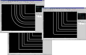
Put HornThis function changes the corner pattern of lead frames, putting out horns of drawing in them as shown below.
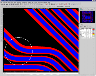
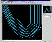
Paraline
It is possible to change the distance from
the baseline, the width of the bunch line, the space between the bunch
lines. As the set-up by the mouse cursor is available, the foregoing
change can be executed instantly by the easy operation.
Correct Pitch
|
Stella Corporation Co., Ltd. |
|||||||||||||||||||||||||||||||||||||||||||


