|
39th NEPCON JAPAN
Light outcoupling technologies of display and ultra-highly transparent
glass were spotlighted
January 22-24, 39th NEPCON JAPAN was held in Tokyo Big Site. In this here,
main topics about electronics are picked up.
Cover glass with low refractive index layer and OLED panel are assembled
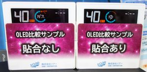
Pic.1 Assemble effect right:without, left:with |
As regards display, OLED maker "SOAR" have run a booth for the first time, and proposed assembled OLED modules.
In this module, cover glass with low refractive index layer was bonded to front of passive matrix OLED panel due to enhance of light outcoupling efficiency. Concretely, a transparent optical resin is coated on cover glass. As a result, light reflection is reduced from 12% to 4% because of air gap-free. And also, light outcoupling efficiency and impression of visual effects are increased because of crisp image quality.
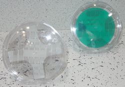
Real display is realized by use of lenticular lens
As concerns same display, Matsaunami Glass Ind exhibited a sparkle display of Innolux Japan. Figure 1 shows image of display mechanism. It's possible to express real image, which is impossible to express by existing display. In short, image is really expressed according to practical visual effects.
|
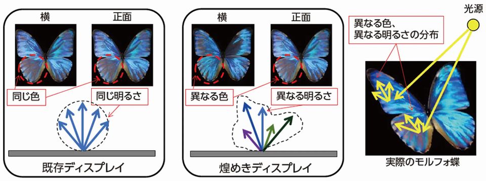
Fig 1. Image of conventional display and sparkle display (from HP of Innolux
Japan)
|
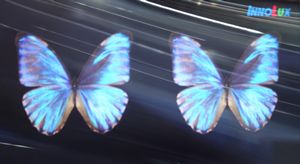
Pic.2 Sparkle Display |
This new display is obtained by setting a lenticular lens on front of TFT-LCD panel. In lenticular lens, UV curing resin are coated on the substrate, and fabricated at fish paste shape by nanoimprinring method. As a result, image is changed by viewing angle, and is expressed at 3D feeling. In a word, real display is obtained like real image. In exhibited 31.5-inch display, lenscular lens of Matsunami Glass was adopted.
Picture 2 shows image of morpho butterfly, is known as emitting of structure color. In this image, visual effects of feather was delicately changed by view angle.
Negative resist is useful for enhance of light coupling efficiency of dispaly
Arakawa Chemical Industries proposed low refractive index type and high
refractive index type negative photoresist as enhance material of light
outcoupling of display, such as OLED. Grain series with Nano size SiO2 and non-grain series are prepared as the former. Refractive index are
1.38 and 1.45 respectively. By contrast, high refractive index type is
composed of ZnO2 and metamorphic group. Its reflective index is 1.68 and over.
3 type can be finely patterned same as L&S = 30μm/30μm. For example, if they are patterned in synchronization with sub-pixel on front of OLED glass as enhancement layer of light outcoupling efficiency, light outcoupling efficiency is greatly increased.
Ultra-high transparent and high hydrophilic glass was spotlighted
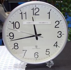
Pic.3 Comparison demonstration of bare glass (left half) and specific fabrication glass (right half) |
NSG group introduced a configurationality Nano porous glass. It's an original porous glass, however, hole diameter becomes to be smaller by gradation in proportion as depth direction. It's possible to wet-etch original soda-lime glass keeping porous property by use of original etchant and optimization of etching process.
Compared to bare glass, firstly, light transmission was increased from 93 % to 96 % in the demonstration test. As a result, light reflection is greatly reduced. In the booth, paper and wall clock with this glass were exhibited. Light reflection and haze were almost not observed.
Furthermore, its surface is very hydrophilic. For this reason, antifouling property is superior because of low contact angle property.
For these reasons, it's effective for cover glass of solar panel, display, and so on.
Conductive film without grain boundary is formed by use of MOD ink
As to conductive material, SIIX introduced metal-organic decomposition (MOD) inks without particle of Electrioninks (USA), and then, appealed to exclusively release in Japan.
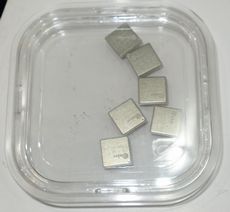
Pic.4 Coated samples of Ag-MOD ink |
This ink is mainly composed of metal complex at ion state. After coating, metal element is precipitated by baking, as a result, it's filmed. As you can image easily, there are not almost grain boundary in this film. In a word, it become s to be like single grain film. For this reason, high specific electric conductivity (90 % of bulk value) is obtained. Baking temperature is 80 - 800 ℃, but above specific electric conductivity is gained by 300 ℃ baking.
Ag, Pt, Ni, Au inks have been released yet, and then, Cu ink will be released in the near future, too.
Fine pattern such as 10 μm is formed by gravure off-set printing
As regards equipment, Seria Corporation appealed gravure off-set printing machine, and then, exhibited main model "PEPIO F6" in the booth.
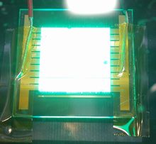
Pic.6 Pilot-produced Green Micro-LED |
Pic.5 Fine pattern sample by the gravure off-set printing |
The company succeeded to directly print fine pattern same as L&S = 10μm/12μm by making use of Cu ink. Picture 5 shows printed samples. Its tact time is approximate 30 sec at 300 × 300 mm substrate.
On the other hand, the company appealed that solder paste could be finely printed, too. Green micro-LED with printed solder paste at 18 μm diameter was exhibited.
|