|
STELLA NEWS SITE is managed by Stella Corporation Inc. |

nano tech 2025 (January 29 - 31, 2025) |
|||||||||
January 29 - 31, 2025, nanotech 2025 was held in Tokyo Big Sight. Main topics are picked up. Firstly, new face "Okura Industrial" announced to enter into perovskite solar cell market, and then, exhibited perovskite solar cells using PET film in the booth.
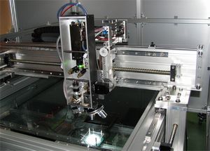
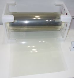
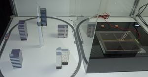
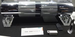
Especially, Ag nano wire film with PET film has been developed as substrate with transparent electrode. Its specific resistance is mere 10 - 20Ω/□, which is lower than that of conventional ITO. Its film can be patterned by existing methods, such as, laser dry etching method and wet etching method using acid series etchant. Of course, bending tolerability is greatly superior. Specific resistance at bending state is not almost degraded. On the other hand, optical transmittance is relatively low, same as, 76 - 82%. As picture 1, it's seemed to be yellowish in fact. In the booth, width sample (300mm) and 100 × 100mm size sample were exhibited. As picture 2, train model was run by power generation, which is generated by perovskite solar cell. By the way, its IPCE (incident photon-to-current efficiency) is not surely estimated yet. The company will enter into the market some sort of state, such as, module maker or device maker. Filgen appealed electron transport material and hole transport material of Sofab Inks As regards material for perovskite solar cell, Filgen introduced original electron transport material and hole transport material of Sofab Inks (USA). The former is mainly composed of Nano size SnO2 grain. IPCE of pilot-produced device was high same as 24 % by making use of this material. Furthermore, its durability is 3 times than that of reference device with C60 ETL. On the other hand, the latter is mainly composed of Nano size NiOx grain. Durability of pilot-produced device is 3 times compared to that of reference device with PTAA. The both are supplied at dispersion liquid, and then, it's pasted at ink state by user side, and coated on the substrate and baked as electron or hole transport layer. By the way, SnO2 dispersion liquid is relatively inexpensive same as 147,000yen/10mL. For this reason, it's possible to reduce ETL manufacturing cost at 30 %. Metal-oxide film is reduced by irradiation of UV light As concerns manufacturing process, Usio proposed reduction treatment technology by irradiation of UV light. In this process, UV light (wavelength 172nm) is irradiated with metal-oxide film in process gas (H2O + H) environment. For example, in case of strong reduction treatment and cleanse at the same time, H2O is more purged. Tact time is mere a few dozen minutes. In the booth, picture of reduced Cu film was exhibited. In short, it's possible to return from metal-oxide film to initial metal film again easily and inexpensively by use of this technology. By the way, its specific resistance of Cu film is not estimated yet. TOYO FPP exhibited high resolution gravure roll for gravure printing
|
|||||||||
| REMARK STELLA NEWS SITE is a free news site of FPD and PCB by Stella Corporation Inc.(This company does not release these FPD and PCB related products.) |
|