STELLA NEWS SITE is managed by Stella Corporation Inc.

SEMICON JAPAN 2024 (Desember 11 - 13)


SEMICON JAPAN 2024 New high adhesive plating process and IJ printing process are proposed

December 11-13, SEMICON JAPAN 2024 was held in Tokyo Big Site. Main topics of device in this exhibition are picked up.

High adhesive property is ensured for glass substrate by use of polypyrrole

Achilles proposed high adhesive plating process using an original polypyrrole paint for glass substrate, which had week adhesive property against upper layer. In this process, this polypyrrole is directly coated on the glass substrate. The next, Pd series catalyst is dipped, as a result, catalyst is held on the uppermost side of the substrate by absorbing of catalyst grain on polypyrrole film. Subsequently, plating film such as Cu, Ni is deposited by non-electrolytic plating using commercial plating solution. Adhesive property is 0.5N/‡o (peel strength). Therefore, it can be used for practical device.


Pic.1 Patterning samples of wet-etching method
This process has high versatility. As above, if polypyrrole film is printed by the screen printing method in advance, plating film is sorbed into polypyrrole pattern only at self-aligning.

And also, polypyrrole film is coated, exposed, developed, plated, and wet-etched by acid, it can be patterned by the conventional wet-etching method. Picture 1 shows sample with patterned Cu line by wet-etching method. As you can easily image, it's possible to form fine pattern easily.

Furthermore, photosensitive polypyrrole paint has been developed for the present moment. In this case, it's possible to form ultra-fine pattern same as line width 3-5 ƒÊm by photolithography (photosensitive polypyrrole coating/exposure/develop/catalyst adsorption/non-electrolytic plating).

By the way, first applications is circuit substrate, interposer, transparent conductive film, and so on.

Fine pattern and thick film can be formed by new IJ ink


Pic.2 IJ printing sample
On the other hand, Sekisui Chemical introduced ultra-fine ink-jet printing method, which was possible to correspond to 3D design. In short, it's possible to print at fine pattern and thick film, for example, 75 ƒÊm line width and 240 - 300 ƒÊm thickness. In fact, high viscosity ink, same as 100 - 1000dPa¥s can be dropped. This value is 10 times than that of conventional IJ ink.

First target is patterning adhesive film and insulation film. In the booth, half-sphere sample with patterned transparent insulator film was exhibited. In the future, the company will enter electrode use.

Micro Technology enters adopts direct exposure process without photo mask

Micro Technology announced to introduce a mask-less exposure system "MX-Series" (Japan Science Engineering), and then, start patterning enterprise by direct exposure process at April, 2025.

It's possible to shorten delivery time and finely and precisely pattern by this direct exposure process, for example, pattern at L&S=3ƒÊm/3ƒÊm, which is difficult to pattern by conventional patterning process using photo mask. However, exposure throughput at 400~400 mm substrate is 10 min and over because of parallel exposure using DLP (Digital Light Processing) method. Therefore, the company will use this process for high-end patterning.

Real like painting display is realized by use of original anti-reflection film


Pic.3 Painting display
As concerns film for display, Daicel exhibited a painting display with an original anti-reflection film. It's a digital painting on display monitor by TFT-LCD, however, texture of color was portrayed, as a result, greatly high quality was obtained. Incident light is scattered reflection by micro-lens fabrication on surface of film. As a result, reflect of incident light does not occur. Therefore, this film can be adopted not only existing applications such as automobile, but also, art applications inclusive of this painting display.


REMARK
STELLA NEWS SITE is a free news site of FPD and PCB by Stella Corporation Inc.(This company does not release these FPD and PCB related products.)

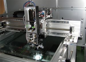
Stella's repair systemgRepair Visionh is suitable for repair use of electrode and so on. Also, it's possible to directly pattern ITO, metal, CNT (Carbon Nano Tube) films by use of this system, too.