 STELLA NEWS SITE is managed by Stella Corporation Inc. |
CEATEC 2024 (October 15 - 18) |
|||||||||||||||||||||||||
October 15 - 18, CEATEC 2024 were held in Makuhari Messe. Main topics are
closed up in this here.
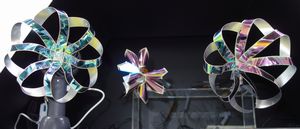
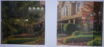
In the booth, basic shape and various flexible shapes were exhibited. Particularly, as picture 2, it's possible to manufacture origami shape device, which is difficult to manufacture in other devices. The company is supplying samples in the present moment, and will to start massproduction at beginning of 2025 by sheet-to-sheet method (not roll to roll method).
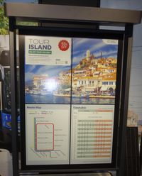
As concerns E-paper display, Sharp exhibited an ultra-large (A0 size) e-poster. Microcapsule type electrophoretic display module were mounted on the glass with TFT. Of course, consumed power is not wasted except for rewriting time of image. As picture 3, solar panel and lamp were set up at upper side, and IoT connect module was set up at lower side. It's possible to rewrite display image at night because of power generation and power storage at daylight, and also, to rewrite at real-time by remote operation. Curtain LED was developed by use of PI film with low-thermal expansion NAGASE exhibited a 100-inch curtain LED "PANELSEMI". It's composed of tiling mini-LED units on Xenomax Japan's original polyimide (PI) film (Xenomax) with low-thermal expansion. It can be housed like a curtain by tiling structure. Of course, it's easy to manufacture rotary type LED because of thin substrate.
Panasonic appeals perovskite solar cell with glass substrates With respect to perovskite solar cell, Panasonic demonstrated prototype with glass substrates. Incident-photon-to-current efficiency (IPCE) is 18.1 %, which is world's best in practical size (30�~30cm).
E-Paper is driven by solution-processed organic-TFT As regards TFT, Yamagata University (Mizukami-Lab) reported to drive 2.1-inch E-Paper displays (146�~240 dot) by solution-processed organic-TFT. It's a bottom gate-bottom contact structure using DTBDT-C6 organic semiconductor. All organic materials inclusive of DTBDT-C6 were deposited by solution process.
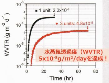
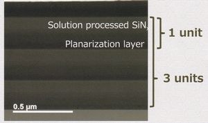
Gas barrier film is formed by densification process Another research group of Yamagata University (Suzuri-Lab) proposed original gas barrier process of solution process and densification process with VUV (vacuum ultraviolet) light irradiation. In this densification process, PDMS (polydimethylsiloxane) is coated, and then, is irradiated N2 and room temperature environment by VUV (172 nm) light, as a result, is changed to SiOx film as planarization layer. On the other hand, PHPS (perhydro-polysirazane) liquid is coated, and then, is irradiated by VUV light, as a result, is changed to SiNx film.
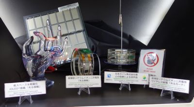
By the way, this stack structure is useful for not only device substrate, but also, encapsulation. In the latter, it's necessary to coat PDMS without solvent firstly, in order to prevent damage against formed organic layers. Transparent conductive film with both advantages of ITO and polymer is developed As concerns material, Murata Manufacturing proposed a newly transparent conductive film as candidate of ITO film.
In the booth, a flexible heater using this film was exhibited. If this film is used, flexible and transparent device can be easily manufactured. |
|||||||||||||||||||||||||
| REMARK STELLA NEWS SITE is a free news site of FPD and PCB by Stella Corporation Inc.(This company does not release these FPD and PCB related products.) |
| Situation of benchmark test We are testing various treatments in respective lacations by using customer's sample substrate always. Situation of benchmark test is this page. |

