STELLA NEWS SITE is managed by Stella Corporation Inc.

The 67th Japan Society of Applied Physics (JSAP) Spring Meeting 2020 (CANCELL)


The 67th Japan Society of Applied Physics (JSAP) Spring Meeting 2020
Transfer processes for a plastic substrate were proposed one after another

Considering the global concerns over the new coronavirus outbreak as well as the press release to event organizers from Japanese Ministry of Health, Labor and Welfare, The Japan Society of Applied Physics (JSAP) decided to cancel the 67th JSAP Spring Meeting 2020, which was scheduled from March 12 - 15 at Yotsuya Campus, Sophia University. In this time, some notice lectures in the proceeding are picked up.

Property of IGZO-TFT is enhanced by high-In IGZO:H film

As concerns oxide-TFT, the research group of Kochi University of Technology announced that the device with high carrier mobility in spite of low manufacturing process was manufactured by high-In IGZO:H film.


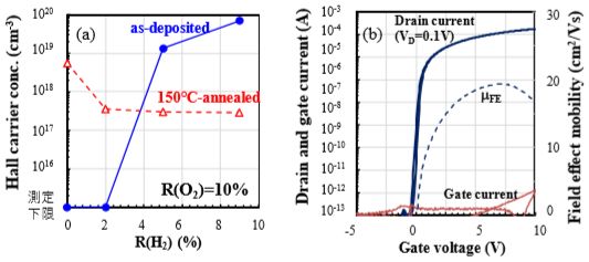
Fig.1 (a) Hall carrier concentration of as-deposited and 150Ž-annealed high-In IGZO:H films deposited at various R(H2), (b) 150Ž-processed high-In IGZO:H TFT with a 20 nm-thick Al2O3 gate insulator1)

In this experiment, high-In IGZO:H films (30 nm) was deposited at O2 ratio = 10 % and H2 ratio = 0 - 9 % by the RF sputtering method. After deposition, its carrier concentration was estimated by hall measuring. As regards TFT, anodically oxidized Al2O3 film (20 nm) and high-In IGZO:H film were used as a gate insulator and a channel respectively. Maximum manufacturing temperature was 150 Ž. Channel width and length were 66/20ƒÊm. All layers were patterned by the conventional photolithography method.

Figure 1-(a) shows hall carrier concentration of as-deposited and 150Ž-annealed high-In IGZO:H film deposited at various R(H2). In as-deposited film, ne was off-scale low at R(H2) … 2 %, on the other hand, it was increased to 1019cm-3 at R(H2) † 5 %. By contrast, after 150Ž annealing, in IGZO film without H, ne was 5~1018cm-3, on the other hand, in IGZO with H, it was 3~1017cm-3. And also, its ne was almost fixed at R(H2) = 2 - 9 %.

Figure 1-(b) shows transfer characteristics of 150Ž-annealed high-In IGZO:H films. Its carrier mobility and S factor were superior (19.4cm2/Vs, 0.13V/dec), too.

Direct photo-patterning process is effective for solution-processed oxide semiconductor inclusive of IGZO

NHK reported effectivity of an original manufacturing process (direct photo-patterning process) for solution-processed oxide semiconductor.

In the experiment, In(NO3), Ga (NO3)3¥xH2O and Zn(NO3)2 were mixed at a certain ratio. It was diluted by pure water and 2-methoxyethanol as a solvent. As a result, a precursor semiconductor liquid was prepared. It was spin-coated on a silicon wafer with thermal oxidized SiO2 gate insulator film. The next, deep UV light was irradiated to its film by the intermediary of a mask due to light oxidation treatment. Subsequently, semiconductor layer was patterned by the wet-etching process, and then, was annealed at atmosphere and 350 Ž. By the way, Mo source/drain electrodes were deposited and patterned by the mask-through evaporation method.


Pic.1 Microscope image of printed and patterned IGZO film by direct photo-patterning method2)
Picture 1 shows microscope image of printed and patterned IGZO film by direct photo-patterning method. The higher water ratio, irradiated areas were uniformly patterned. And also, manufactured TFT using water solvent had a superior property. For example, its carrier mobility was 5.0 cm2/Vs, which was almost same as that of patterned TFT by the conventional photolithography. Furthermore, in other oxide semiconductorCsuch as IZO and InO, if water was used as a solvent, superior characteristics of TFT were obtained, too.

In short, it's advantageous for this patterning method to use water solvent. Its reason why a hydroxyl radical is generated by photodecomposition of water, and it operates effectively as an oxidant.

c-Si films on a silicon wafer are repeatedly transferred to plastic films

With respect to TFT for flexible devices, the research group of Hiroshima University reported a unique transfer process, which is possible to transfer repeatedly high-quality crystal silicon (c-Si) film to surface of plastic substrates.


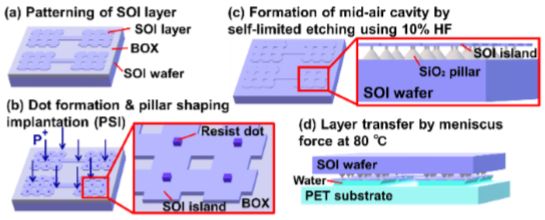
Fig.2 Schematic diagram of MLT process3)

Figure 2 shows schematic diagram of MLT (Meniscus force-mediated Layer Transfer) process, which was originally developed. First of all, SOI (Silicon on Insulator) layer was patterned at dog bone shape due to forming hollow structure. The next, PSI (Pillar Shaping Implantation) treatment was done at 1.0~1014, 130keV, as a result, fine SiO2 pillars were formed as a photoresist dot mask pattern. Subsequently, BOX (Buried Oxide) layer was wet-etched by use of 10 % HF, as a result, SiO2 pillars were formed. It supports c-Si film with hollow structure. This c-Si film and PET film were contacted face-to-face, and annealed at 80 Ž. As a result, c-Si film is transferred to PET substrate in low temperature environment by strong meniscus force, which operates as attraction of the both substrates.


Fig.3 Schematic diagram of local transfer3)

Figure 3 shows schematic diagram of local transfer. First of all, non-transfer area in PET substrate was treated to hydrophobic property by deposition of hydrophobic film (30 nm), on the other hand, transfer area (400 ~ 400 ƒÊm) was treated by UVO3 treatment. As a result, it became to be hydrophilic. After PET substrate was dipped into pure water, and pulled out, pure water was located to hydrophilic area selectively. Located transfer is completed by contacting the both substrates face-to-face in this state.


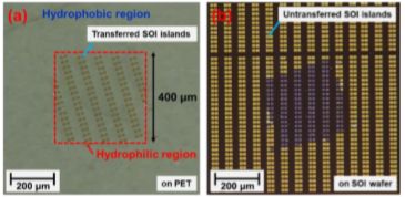
Pic.2 Optical microscope images of (a) locally transferred SOI islands on PET and (b) removed SOI islands on the initial SOI wafer3)
In this time, contact angle of hydrophobic area and hydrophilic area were 114‹ and 30‹ respectively. Above selective transfer process is realized by this large difference. As picture 2 indicates that non transfer c-Si film keeps initial shape without damage. For this reason, itfs possible to transfer c-Si pattern from single SOI wafer to some plastic substrates repeatedly. By the way, process time of local transfer process was approximate 20 sec. In short, c-Si device can be manufactured on plastic films at high yield, low cost, and high throughput by making use of this process.

Small-molecular semiconductor film is coated on hydrophobic Cytop gate insulator film

As regards organic-TFT, the research group of University of Tokyo and National Institute of Advanced Industrial Science and Technology (AIST) succeeded to coat an amorphous small-molecular film on Cytop gate insulator film, which is easy to coat dense film on surface because of low surface energy.


Fig.4 (a) Crossed-Nicols polarized micrographs of printed organic crystals on top of Cytop. (b) Schematic of bottom-gate bottom-contact-type TFT. (c) Transfer characteristics of printed TFT (W/L = 800 ƒÊm/100 ƒÊm, Ci = 24 nF/cm2). (d) Gate voltage dependency of subthreshold swing (SS)4)

In this time, a sheathed crystal material gPh-BTNT-Cnh was used as a small-molecular semiconductor material. Its liquid was coated by the blade coating method, which liquid was swept to a certain direction. As figure 4-(a), it's confirmed that coated film on Cytop film was a crystal thin film with single crystal domain (a few mm2 size) by crossed Nichol observation. It's possible to adopt this process in not only flat surface, but also, non-flat surface with source/drain electrode, too. Therefore, in this time, a bottom-gate bottom-contact type TFT was manufactured by use of evaporated Au source/rain.

Pilot-produced device was driven at 2 V and under. Hysteresis phenomenon was not observed. And also, carrier mobility was relatively high same as 4.4 cm2/Vs. Furthermore, high steep switching property same as average 72 mV/dec was obtained in sub-threshold region. This value is near to theoretical limitation.

High carrier mobility organic-TFT is manufactured by a new transfer method


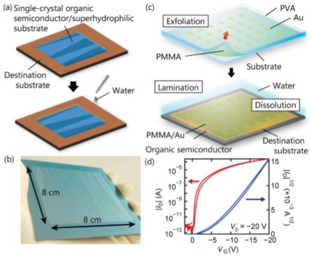
Fig.5 (a) Schematic illustration of the transfer method for semiconductor film. (b) Photograph of an 8 ~ 8 cm sized C9-DNBDT-NW film. (c) Schematic illustration of the transfer method for electrodes. (d) Transistor characteristic of the fabricated monolayer OFET (L/W = 200 ƒÊm/1000 ƒÊm)5)

On the other hand, the research group of University of Tokyo, National Institute for Materials Science (NIMS), JST, and PI-CRYSTAL reported a new transfer process in order to extend degree of freedom of manufacturing process.

As figure-(a), a single crystal film is transferred to a glass substrate with ultra-hydrophobic property by utilization of their surface energy difference and making use of water. First of all, a single crystal film of p-type semiconductor "C9-DNBDT-NW" could be coated on large area (8 ~ 8 cm). By contrast, electrodes were patterned on a glass substrate with separation layer, and then, thin PMMA layer and thick & soluble polymer PVA layer were coated on electrodes, finally it's released. As a result, electrode film is manufactured. This film is laminated on single crystal filmCand then, dissolved into water. As a result, electrode film and semiconductor film are joined by electrostatic force of PMMA. For this reason, an organic-TFT with high carrier mobility (10 cm2/Vs) can be manufactured by use of single crystal film.

Nanocarbon film is transferred and patterned to a plastic substrate by laser irradiation

As concerns Nano size carbon, the research group of Tokyo University of Science announced a new transfer and direct patterning process of carbon nano tube (CNT) for a plastic substrate by laser irradiation.

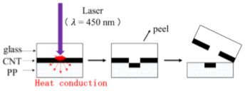
Figure 6 shows fabrication process. First of all, MWNT (Multi Wall Nano Tube) is coated on the glass substrate at 150 Ž by the spray deposition method. By the way, a commercial product (Meijo Nanocarbon MW-‡T) was used as a MWNT bulk material. The next, this glass substrate and a polypropylene (PP) film are contacted. Subsequently, CW laser (wavelength 450 nm) was irradiated to this sample from glass side.


Pic.3 Relationship between line width and laser power6)


Fig.6 Fabrication process of MWNT pattern on PP film6)

As a result, in irradiated area, MWNT electrode is formed on surface of PP film by composition of MWNT and PP. Picture 3 shows relationship between line width and laser power. As you know, it's possible to control line width by laser power. In this experiment, minimum line width was 30 ƒÊm. Furthermore, line width could be controlled by fabrication speed. And also, it's confirmed that not only MWNT, but also, single wall nano tube (SWNT) and graphite carbon could be transferred by this process, too.

Reference
1)Furuta, et.al.FLow temperature fabrication of high mobility hydrogenated InGaZnOx thin film transistors, The 67th JSAP Spring Meeting, 2020, 15-005 (2020.3)
2)Miyakawa, et.al.FDirect Photo-patterning Process for Solution-processed Metal Oxide TFT, The 67th JSAP Spring Meeting, 2020, 15-008 (2020.3)
3)Hirano, et.al.FDevelopment of Local Transfer Process of Single-Crystalline Silicon Thin Films on Plastic Substrate, The 67th JSAP Spring Meeting, 2020, 11-375 (2020.3)
4)Kitahara, et.al.FThin-Film Coating of Small-Molecule Semiconductors on Cytop Gate Dielectric and Highly Sharp TFT Switching, The 67th JSAP Spring Meeting, 2020, 10-347 (2020.3)
5)Makita, et.al.FFabrication of Organic Single-crystal Transistors by Transfer Techniques, The 67th JSAP Spring Meeting, 2020, 10-346 (2020.3)
6)Isomae, et.al.FFabrication of nanocarbon patterns by laser thermal transfer method, The 67th JSAP Spring Meeting, 2020, 14-006 (2020.3)


REMARK
STELLA NEWS SITE is a free news site of FPD and PCB by Stella Corporation Inc.(This company does not release these FPD and PCB related products.)

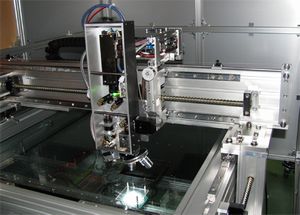
Stella's repair systemgRepair Visionh is suitable for repair use of electrode and so on. Also, it's possible to directly pattern ITO, metal, CNT (Carbon Nano Tube) films by use of this system, too.