The 85th JSAP Autumn Meeting, 2024
New proposals for perovskite solar cell occur one after another
September 16 - 20, The 85th JSAP Autumn Meeting, 2024 was held in Toki
Messe and other surrounding facilities. Topics of OLED, oxide-TFT, and
perovskite solar cell are closed up.
WF of EIL is reduced for flexible OLEDs by using organic strong base
As regards OLEDs, the research group of Chiba University, NHK, Nippon Shokubai,and
Osaka University reported flexible OLEDs using specific electron injection
materials, which were not easy to degrade against H2O.
As you know, electronic affinity of OLED emitting material is 2.5 eV and under. For this reason, alkali metals are used as EIL because of low WF (3 eV and under). However, device lifetime is limited by alkali metal because of high reaction, and also, practical use is difficult in case of using of flexible substrate, such as rubber sheet and plastic film.
Therefore, the research group has developed new electron injection materials
with low WF instead of alkali metal. Firstly, WF was reduced to 3.0 eV
by making use of hydrogen bond between organic strong base and other organic
semiconductor. Furthermore, WF of ZnO neighborhood was to 2.4 eV by coordinated
reaction between ZnO and N2 in phenanthroline derivative. In short, WF of Al was reduced from 4.1
eV to 2.0 eV by use of strong base, was possible to adopt both reactions.
This value is same as that of Cs, is lowest WF in all alkali metals.
Nippon Shokubai pilot-produced flexible OLEDs using this technologies.
In this device, simple gas barrier film (10-4g/m2/day) was used for encapsulation. It's emitted continuously, After 3000
h, image quality was not degraded. In short, it's easy to correspond to
full flexible OLEDs using soft and flexible film and substrate.
|

Fig.1 (a) Schematic illustration of change in WF caused by strong bases.
(b) Pictures of flexible OLEDs1)
|
Poly IGO-TFT is suitable for all OLEDs because of high carrier mobility and durability
As regards TFT, Japan Display introduced poly-crystalline Oxide Semiconductor(Poly-OS-TFT) as a new oxide-TFT.
In poly-OS-TFT, polycrystal InGaO is used as oxide semiconductor. It's high carrier mobility same as 50 cm/V・s and over and low leak current. In short, it's advantages of poly-Si TFT and conventional IGZO-TFT. Furthermore, it's possible to mass-produce by use of ultra-large mother glass, same as G6 size (1500 × 1800 mm). By the way, IGO is poly-crystallized by solid-phase growth at 350 - 400 ℃ anneal.
Figure 2 shows characteristics of oxide-TFTs on G6 mother glass. Carrier mobility of poly-IGO-TFT is 5 times and over compared to that of conventional IGZO-TFT. And also, it's improve bias stress durability by optimization of manufacturing process. Furthermore, channel width and length dependence is not almost. In short, if channel dimension is fine such as W/L = 1.5 μm/1.0 μm, carrier mobility is almost changed from value of W/L = a few μm.
|

Fig.2 Characteristics of oxide-TFT on G6 mother glass (1500 × 1800 mm)2)
|
H doped poly-InOx:H-TFT is advantageous for high carrier mobility and low Vth shift
On the other hand, Kochi University of Technology reported H doped poly-InOx:H-TFT with high carrier mobility and high reliability.
In this experiment, bottom gate-etching stopper type poly-InOx:H-TFT was manufactured on 4-inch glass substrate. Poly-InOx:H film was poly-crystallized by solid-phase growth at 300 ℃. Figure 3 shows annealing temperature dependence (a), TFT transfer characteristics (b), and NBTS reliability (c).
The next, PE-CVD deposited SiOx:H film and IPC-CVD deposited H-free SiOx
film were formed as etching stopper,due to influence of H diffuse. Carrier
mobility of SiOx:H and H-free SiOx devices were 45 cm2/V・s and 29.9 cm2/V・s, and Vth were 0.18 V and 0.23 V respectively. In short, if H was doped
into SiOx film, TFT characteristics was enhanced.
On the other hand, PBTS (Positive Bias Temperature Stress) and NBTS (Negative Bias Temperature Stress) of H-free SiOx TFT was superior compared to SiOx:H TFT. This is reason why in case of H-free, device reliability is improved because of increase of film density.
|

Fig.3 Annealing temperature dependence of (a)TFT transfer characteristics
and (b) Vth; (c)NBTS reliability3)
|
Characteristics of perovskite solar cell is improved by use of hole-collecting monolayer materials
With respect to perovskite solar cell, Kyoto University proposed to use self-assemble monolayers (SAM) as hole-collecting materials, due to block of electron and absorption of hole.
In previous time, the research group reported 3PATAT-C3 as hole-collecting monolayer materials, and also, pilot-produced a device with relatively high IPCE same as 23 %. However, it's difficult to coat perovskite film on substrate uniformly because of strong hydrophobic property.

Fig.4 (a) Molecule structure of 4PATTI-C3, (b) J-V curve of perovskite
solar cell using 4PATTI-C3 film4)
|
Therefore, in this time, tetrapod type hole-collecting monolayer material "4PATTI-C3 (figure 4-(a))" with 4 phosphonate groups was synthesized due to strong adsorption force against metallic oxide surface. And then, DMF solution inclusive of 4PATTI-C3 was spin-coated on glass substrate with ITO film. As a result, SAM was formed on ITO electrode.
Figure 4-(b) shows J-V curve of perovskite solar cell using 4PATTI-C3 film. In case of using perovskite material with almost same as valance band (VB) level (-5.58eV) of HOMO level of 4PATTI-C3, IPCE was 19.3 %. On the other hand, in case of perovskite material with deep VB level (-5.69 eV), IPCE was greatly increased to 21.7%.
This is reason why 4 phosphonate groups adsorb into ITO and perovskite by anchor effect, and also, wettability is greatly improved because of low contact angle (40°).
IPCE is increased by co-coating of SAM and perovskite
On the other hand, Saitama University reported that IPCE of perovskite solar cell was furthermore increased by co-coating SAM-HTL and perovskite material.
|

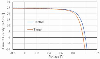
Fig.6. J-V curves of PSCs in reverse scan mode5)
|
|

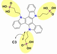
Fig.5. The structure of 3PATAT-C35)
|
SAM with multiple bonding anchors "3PATAT-C3 (figure 5)" was doped into perovskite precursor solution. And then, it's coated on glass substrate with ITO film. As a result, SAM-HTL and perovskite layer were co-coated in the same time. Target device was produced by stack of PC61BM, BCP, and Ag. By the way, SAM-free device and SAM-HTL and perovskite sequential device (Control) were pilot-produced respectively due to comparison.
IPCE of SAM-free device was 10.1 %, on the the hand, that of control device was 17.6 % because of increase of Joc, Voc, and FF. Furthermore, that of target device was maximum 20.4 % at 3PATAT-C3 0.75mmol/L doping. If doping ratio is 2.1 mmol/L, IPCE was not changed at 20.4 %. This is reason why film form is degraded by excess doping.
Improvement characteristics of perovskite deive by alkali metal hydroxide is researched
|

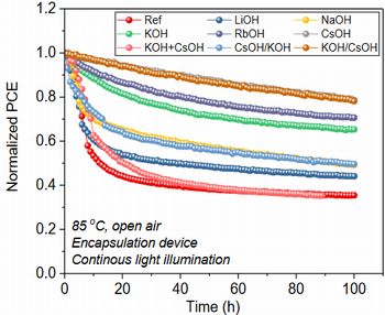
Fig.8 High-temperature endurance6)
|
|

Fig.7 IPCE6)
|
The research group of Kyushu University reported surface treatment effect
of SnO2 electron transport layer (ETL) in perovskite solar cell by alkali metal
hydroxide.
In this experiment, surface of SnO2-ETL were treated by use of LiOH, NaOH, KOH, RbOH, and CsOH. If LiOH, NaOH,
and KOH were used, initial efficiency was increased, on the other hand,
high-temperature endurance (light irradiation + 85 ℃) was deteriorated
(figure 7, 8). As a result, film quality of perovskite was enhanced, and
also, electron extraction efficiency was increased by these treatments.
By contrast, in case of RbOH and CsOH, initial efficiency was decreased,
on the other hand, high-temperature endurance was improved (figure 5, 6).
The next, surface treatment of KOH + CsOH and continuous treatment of KOH
→ CsOH (KOH/CsOH) and CsOH → KOH (CsOH/KOH) were tried. As a result, if
device was treated by KOH firstly, and then by CsOH secondly (KOH/CsOH),
IPCE and high-temperature endurance were enhanced, too (figure 7, 8).
Sputtered and annealed SnO2 is effective for electron transport layer of perovskite solar cell
The research group of NAIST and Aoyama Gakuin University proposed SnO2 with superior optical and electrical characteristics as electron transport
material instead of conventional TiO2, and also, shown to be able to correspond to large substrate by sputtering
deposition of SnO2 film.
|

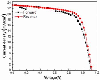
Fig.9 J-V curve of device with annealed SnO2-ETL at 400 ℃7)
|
In this experiment, SnO2 films were deposited on glass substrate with ITO film at 40 nm thickness,
and then, annealed at 300 ℃, 400 ℃, 450 ℃ and 500 ℃. The next, FAPbI3 and Spiro-OMeTAD were spin-coated as perovskite layer and hole transport
layer respectively. Finally, Au electrode was evaporated at 80 nm thickness.
Figure 9 shows J-V curve of device with annealed SnO2-ETL at 400 ℃. In this device, JSC, VOC, and IPCE were 23.28 mA/cm2, 1.126 V, and 18.22 % respectively. These values was highest in these pilot-produced devices. This is reason why optical bandgap is changed by anneal temperature.
Originally transparent PI film is used for flexible substrate of perovskite solar cell
I.S.T Corporation and Toin University of Yokohama proposed originally transparent polyimide film "TORMED" for flexible substrate of perovskite solar cell. TORMED is a transparent PI film with high durability and thermal resistance, and then, is expected as a flexible substrate instead of PET film and conventional PI film.
|

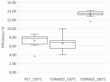
Fig.10 Relationship of anneal temperature and distribution of IPCE after
coating SnCl28)
|
In this experiment, SnO2 films, CH3NH3PbI3 film, and spiro-OMeTAD film were spin-coated on TORMED. By the way, SnO2 film was obtained by coating of SnCl2・2H2O ethanol solution and annealing.
Figure 10 shows relationship of anneal temperature and distribution of
IPCE after coating SnCl2. Average IPCE of 150 ℃ annealed PET sample and TORMED sample was almost
same as 7 %, on the other hand, that of 180 ℃ annealed TORMED sample was
13 %, and also, distribution of IPCE was greatly enhanced. This means that
excellent SnO2 film is obtained by 180 ℃ anneal. In short, if TORMED is used as substrate,
materials and manufacturing process of glass substrate device can be diverted
because of high thermal resistance.
Fine Ag mesh electrode is formed by laser induced photoreduction method
As concerns next generation touch panel, Shizuoka University proposed fine Ag mesh electrode as flexible transparent electrode by laser induced photoreduction method due to invisible by bare eyes.
As figure 11-(a), it's easy to control sheet resistance and transmittance
of Ag mesh electrode because of laser induced deduction method without
mask. A polymer with polyimide precursor and silver nitrate was used as
photoreduction material.
In this experiment, blue laser (wavelength 405 nm) was locally irradiated
to polymer, and then, Ag electrode was formed by reduction of Ag ion. Minimum
line width was 2 μm. And also, minimum resistance same as 2.2 × 10⁻⁷ Ω・cm was obtained in 7 mW laser power and 200 μm/s drawing speed.
|

Fig.11 (a) Fabrication of silver mesh pattern by laser induced photoreduction. (b) The SEM image of the fabricated silver line. (c) Photo of silver mesh transparent electrode9)
|
Reference
1)Fukagawa, et.al.:Development of low work function electrodes using organic strong bases and their application to flexible OLEDs, The 85th JSAP Autumn Meeting, 2024, 100000001-018 (2024.9)
2)Tsubuku, et.al.:Cutting-edge backplane technologies for OLED display, The 85th JSAP Autumn Meeting, 2024, 100000001-333 (2024.9)
3)Okamoto, et.al.:Highly Reliable Bottom Gate Poly-InOx:H Thin-Film Transistor, The 85th JSAP Autumn Meeting, 2024, 100000001-334 (2024.9)
4)Truong, et.al.:Cyclooctatetraene-based Hole-Collecting Monolayer Materials for Perovskite Solar Cells, The 85th JSAP Autumn Meeting, 2024, 11-128 (2024.9)
5)Tomita, et.al.:Perovskite Solar Cells via Simultaneous Formation of Hole Transport Layer and Perovskite Layer with multiple bonding anchors, The 85th JSAP Autumn Meeting, 2024, 11-398 (2024.9)
6)Matsushima, et.al.:Higher-Performing Perovskite Solar Cells Treated with Alkali Metal Hydroxide, The 85th JSAP Autumn Meeting, 2024, 11-409 (2024.9)
7)Ogawa, et.al.:Sputter processed SnO2 films for perovskite solar cell applications, The 85th JSAP Autumn Meeting, 2024, 11-320 (2024.9)
8)Takasuka, et.al.:Fabrication of perovskite solar cell using transparent polyimide film as a base material, The 85th JSAP Autumn Meeting, 2024, 11-329 (2024.9)
9)Shimada, et.al.:Development high-definition silver mesh transparent electrode by blue semiconductor laser induced photoreduction, The 85th JSAP Autumn Meeting, 2024, 11-046 (2024.9)
|


