|
|
STELLA NEWS SITE is managed by Stella Corporation Inc. |

|
FPD/PCB NEWS〜January 30
|
|
NEG officially adopted for the new glass dome tweeter released by SEAS Nippon Electric Glass (NEG) announced that the ultra-thin glass diaphragm jointly developed with GAIT, a glass processing company in Taiwan, has been officially adopted for the new glass dome tweeter (T27GL001 DXT) released by SEAS, a world-renowned speaker unit manufacturer based in Norway.A glass dome tweeter is a speaker component that reproduces high frequency sound using a dome shaped glass diaphragm. The T27GL001 DXT is the first SEAS model to incorporate a glass diaphragm and utilizes NEG's ultra-thin glass, which is extremely thin and lightweight while offering exceptional strength. Thanks to these material properties, the tweeter delivers extremely fast sound attack and clearly reproduces even subtle sonic details. Glass is also resistant to humidity and deterioration over time, enabling long term stability in sound quality. |
|
FPD/PCB NEWS〜January 29
|
|
Stanley Electric acquires all shares of Iwasaki Electric to make it a consolidated subsidiary Stanley Electric announced to resolve at its board of directors meeting held today to acquire all shares of Iwasaki Electric to make it a consolidated subsidiary. |
|
FPD/PCB NEWS〜January 26
|
|
Ricoh Signs Agreement with Saitama City on Demonstration Project for CO2 Sensors Equipped with Perovskite Solar Cells Ricoh Company and Ricoh Japan have signed an agreement with Saitama City regarding a demonstration project for CO2 sensors equipped with perovskite solar cells.Under the demonstration project, CO2 sensors will be installed in the Saitama City Main Government Building from January 2026 to March 2027 to collect data on temperature, humidity, CO2 concentration, illuminance, and the heat index. By utilizing this data, the project aims to widely promote Saitama City's initiatives for the use of perovskite technology, as well as to verify the power generation performance and durability of the CO2 sensors through data collection, analysis, and evaluation. |
|
FPD/PCB NEWS〜January 21
|
|
|
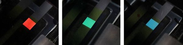
NHK Succeeds in Developing World's First Blue-OLED that also Generates Power
This pioneering development was achieved by using MR-TADF materials that combine high luminous efficiency for light emission and strong light absorption for solar power generation, and by precisely controlling energy within the device. For display applications, the research team achieved red, green, and blue emission, with blue emission marking a world-first for a dual-function device, and therefore, enabling emission of a wider range of colors. |
|
FPD/PCB NEWS〜January 14
|
|
UBE and Tohoku University Establish the Co-creation Research Institute for Future Driven Technologies UBE Corporation and Tohoku University have established the "UBE x Tohoku University Co-creation Research Institute for Future Driven Technologies " within the Institute of Multidisciplinary Research for Advanced Materials (IMRAM), Tohoku University and commenced operations on January 1, 2026. |
|
FPD/PCB NEWS〜January 13
|
|
|
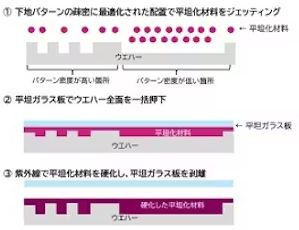
Canon achieves world first with novel inkjet-based wafer planarization, delivering dramatically smoother wafer surfaces
Canon developed a nanoimprint lithography method in which an inkjet system is used to apply resist onto wafers before a patterned mask is pressed onto the surface like a stamp to transfer circuit patterns. Canon then incorporated this technology into the FPA-1200NZ2C semiconductor manufacturing system, launched in October 2023. Building on this foundation, Canon developed IAP by adapting key elements of nanoimprint lithography for use in the planarization process. An inkjet is used to dispense light-curable material onto areas of the wafer in a precisely tuned manner that matches surface topography, including the distribution of circuit patterns. High-precision planarization is achieved by then pressing a flat glass plate onto the wafer. This makes it possible to precisely level the entire surface of a 300 mm-diameter wafer in one stamping process, regardless of variations in the underlying circuit design or topographical density. Topographical irregularity is thereby reduced to 5 nm or less, facilitating the uniform layering of structures essential for subsequent downstream processing. |
|
FPD/PCB NEWS〜January 9
|
|
|
Tokyo Metropolitan Bureau of Transportation Launches Pilot Program Introducing AI-Powered Transparent Translation Displays on Toei Buses
The new building will have a total floor area of about 20,000 square meters and is intended to strengthen production capacity for interchangeable lenses for digital cameras, high-performance objective lenses for microscopes, projection lenses for semiconductor lithography equipment, and industrial lenses. Nikon aims to promote new manufacturing practices, including the renewal of production lines, the introduction of mixed-model production, and the automation of in-building logistics. |

|
FPD/PCB NEWS〜January 6
|
|
|
Tokyo Metropolitan Bureau of Transportation Launches Pilot Program Introducing AI-Powered Transparent Translation Displays on Toei Buses Transparent displays will be installed around the driver's seat to evaluate their effectiveness and convenience in facilitating communication with a diverse range of passengers. The trial period will run from January 15 to 29. |