|
STELLA NEWS SITE is managed by Stella Corporation Inc. |

Innovation Japan 2023 (August 24 - 25) |
||||||
August 24 - 25th, Innovation Japan 2023 was held in Tokyo Big Site. New topics with focus on perovskite solar cell are closed up.
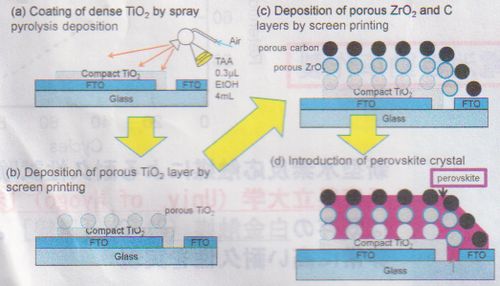
Its original technologies are device structure and manufacturing process. As figure 1, dense TiO2 film is spray-coated on glass substrate with FTO transparent electrode, and then, porous TiO2 is printed by the screen printing method, and then, annealed at 500üÄ. The next, porous ZrO2 and porous carbon electrode are printed, and then, annealed at 400üÄ. Finally, Pb series perovskite liquid is injected into above porous layers, and sorbed.
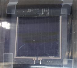
And also, device durability is superior because of high water resistance of carbon electrode. In fact, sufficient durability same as 3000 h was obtained at 85üÄ, 85%RH environment. This value means maker guarantee is 10 years or over. By the way, ICPE is approximate 12 %. In the booth, 80ü~80ćo sample and small samples were exhibited. This device has been practical use yet. By the way, glass should be used as a substrate because of above process temperature. In short, it's not possible to realize a flexible device using a plastic film. Durability and efficiency are enhanced by polysilane treatment
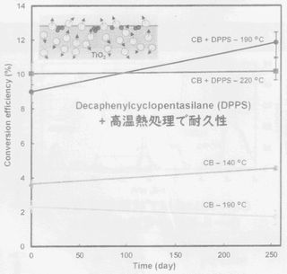
In this experiment, FTO film, dense TiO2 film, porous TiO2, and CH3NH3PbI2 perovskite film were deposited, and then, DPPS polysilan was spin-coated, and then, annealed at 140 - 220üÄ. The next, Spiro-OMeTAD film was spin-coated, and then, Au film was evaporated. Figure 2 shows comparison of IPCE. IPCE of device with treated by chlorobenzene (CB) was relatively low, on the other hand, that of device with CB + DPPS was greatly higher than that of CB device. Furthermore, if the device was annealed at 220üÄ, IPCE was not almost changed. In short, high durability was obtained. Water resistance of PVK device is improved by use of PVK solution Saga University tried to coat PVK film by use of water solution, in order to enhance water resistance of PVK device. In general, PVK is stable into high density halogenated methylamine. For this reason, water solution inclusive of PVK is used: as a result, water resistance of device was enhanced. In short, it's unnecessary to form gas barrier layer or strong encapsulation film in general. However, its IPCE was relatively low same as 3%. This value is that of simply sample device (ITO/TiO2/PVK/electrolyte/Au). In short, if device structure is optimized by insert of carrier transport layer and optimization of material and layer, IPCE is expected to be increased to 2 times or over. Nano mist using plasma has many applications
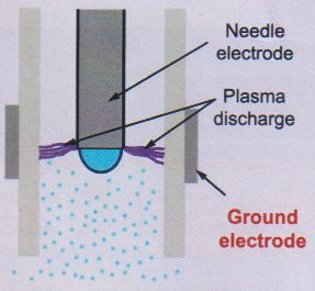
As figure 3, various liquids are changed to Nano size mist state by the plasma Nano mist generation system, and then, sprayed on the object. It's possible to change various liquids, such as oil series, water series, to Nano mist state. For example, furtherance of transdermal absorptionanesthetic, increase of combustion efficiency of petrol, sterilization of agricultural crops, and so on. In the field of electric device, it's effective for deposition of Nano size thin film. In this case, it's easy to coat dense and flat thin film. |
||||||
| REMARK STELLA NEWS SITE is a free news site of FPD and PCB by Stella Corporation Inc.(This company does not release these FPD and PCB related products.) |
Novel system was released as manufacturing system of emulsion film mask. |