|
STELLA NEWS SITE is managed by Stella Corporation Inc. |

Innovation Japan 2020 - Online (September 28 - November 30) |
||||
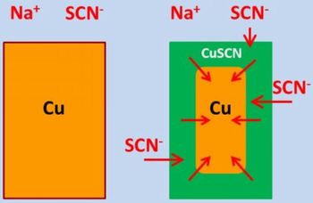
September 28th, Innovation Japan 2020 - Online has started by the online method. Many demonstrations are disclosed until November 30th by a specific homepage. Topics for electronics device are closed up based on the homepage. Cu electrode with high work function is gained by dipping treatmentKyushu Institute of Technology proposed low-cost organic electronic devices with Cu electrodes.
Effective application is organic transistor with bottom gate/bottom contact structure. In fact, an organic transistor was pilot-manufactured by making use of this technology as source/drain electrode (L&S = 100 μm/20 μm). Organic transistor with low contact resistance could be formed by low cost. Beyond that, it's effective for anode and hole transport layer of OLED and organic solar cell. Ultra-fine Ag pattern is formed by direct laser irradiation
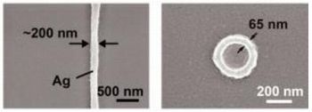
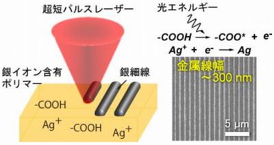
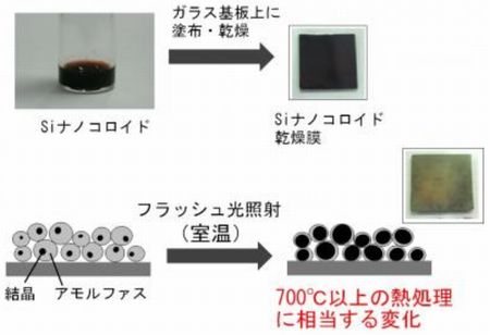
As figure 2, a femtosecond pulse laser is irradiated with a polymer film with dissolved Ag ion. In this time, carboxyl group in polymer absorbs light. As a result, an electron is emitted. Ag ion catches this electron; as a result, it's precipitated by reduction. Metal is precipitated to laser irradiated area only because of light reduction. In short, fine pattern can be obtained at will by laser scanning. Figure 3 shows microscope image of Ag line and nanosized Ag ring. In short, it's possible to obtain ultra-fine line such as a few dozen nm easily. Nano-silicon is crystalized at RT by irradiation of flash light University of Hyogo introduced a photo-crystallizing nano-silicon inks. It's crystallization technology of nanosized silicon ink by light irradiation treatment instead of conventional anneal treatment. This technology can be adopted for low thermal resistance substrate such as various plastic films.
It's possible to enhance crystalline nature of Ag grain for low thermal resistance substrate such as plastic films because of RT environment process. In fact, substrate temperature in this process was 40 ℃ and under. |
| REMARK STELLA NEWS SITE is a free news site of FPD and PCB by Stella Corporation Inc.(This company does not release these FPD and PCB related products.) |
Novel system was released as manufacturing system of emulsion film mask. |