|
STELLA NEWS SITE is managed by Stella Corporation Inc. |

Innovation Japan 2019 (August 29-30, 2019) |
||||||||
August 29-30, Innovation Japan 2019 were held in Tokyo Big Sight. New topics of manufacturing process in this exhibition are picked up.
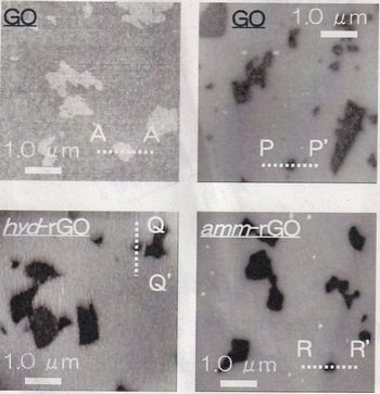
Of course, it's possible to pattern graphene film by use of photolithography methods using graphene dispersion liquid for fine patterning. After patterning, graphene film is removed finally. Compared to the dry etching method, process damage can be greatly reduced, on the other hand, compared to the conventional wet etching method, anisotropic aspect and etching depth are higher, as a result, it's easy to form pattern with high aspect ratio. And also, as picture 1, it's possible to control etching depth by kind of graphene sheet, such as, hyd-rGO, GO, and amm-rGO. By the way, etching rate is very low, same as a few dozen nm/h at the present moment. Support carrier mobility and driving stability of oxide-TFT by homo stacking structure
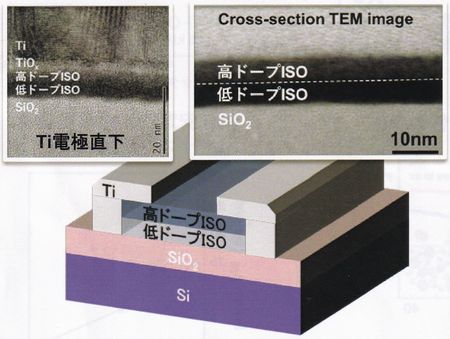
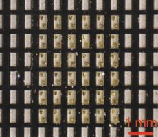
Its carrier mobility is high same as 17.4 cm2/Vs, which is higher that of the conventional IZGO-TFT. Furthermore, driving stability is superior, such as ΔVon=0.2V, and also, ON/OFF current ratio is 107 and over. Of course, ISO films can be deposited at low temperature (RT - 250℃) by the conventional sputtering methods, and patterned by the conventional photo-etching method, too. μLEDs are integrated by direct etching of the substrate The research group (Prof.Honda, et.al.) of Kogakuin University reported integration technology of μLED, which is a next generation direct imaging display.
|
||||||||
| REMARK STELLA NEWS SITE is a free news site of FPD and PCB by Stella Corporation Inc.(This company does not release these FPD and PCB related products.) |
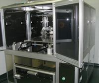
Novel system was released as manufacturing system of emulsion film mask. |