JPCA Show 2019 Demonstrations of Ag paste for the screen-printing were
cranked-up
June 5-7, JPCA Show 2019 was held in Tokyo Big Sight. Main topics in this
exhibition are picked up.
 |
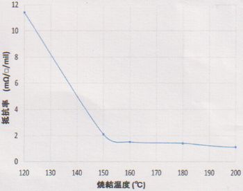
| Figure 1. Relationship of annealing temperature and specific resistance |

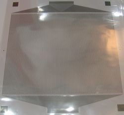
Picture 1. Printed sample on the PET film
|
As concerns Ag paste for the screen-printing method, firstly, Mino Group introduced GENSEINK's Nano Ag paste“Smart Screen”. It's composed of Nano Ag grain (diameter = approximate 100 nm) and organic solvent. In short, a binder is not contained. Therefore, compression stress against the substrate does not occur in annealing process, as a result, warpage and crinkle are not generated in thin plastic film. In this time, PET film (t = 25 μm) based sample was exhibited. Furthermore, it's possible to correspond to thinner film, for example t = 100 μm class.
And also, as figure 1, relatively low specific resistance is obtained by low temperature annealing process (120 - 180℃) because of high concentration (55 %). Compared to the conventional μm size Ag paste, film thickness is approximate 1/5, but specific resistance is approximate 1/2. However, it's not suitable for fine pattern because of low printing resolution. By the way, Mino Group sells this paste as an agent.

Picture 2. Printed sample for touch panel
|
By contrast, Toyo Ink demonstrated a μm size Ag paste "REXALPHA RA
FS 059". It's suitable for continuous printing process, in short,
mass production because of excellent patterning repeatability. Standard
printing resolution is L&S = 50μm/50μm. However, if an original anchor
material "RA AC 001" is used for under layer, this Ag film can
be fine same as L&S = 30μm/30μm because of suppression of bleeding
in the printing process. By the way, volume resistivity of printed film
is 4×10⁻⁵Ω・cm.
A new face entered into the gravure cylinder mask market
With respect to infrastructure for gravure printing, Athene announced to enter into the gravure cylinder mask market. In this introduced prototype, Ni film is deposited and patterned by electroforming process. For this reason, patterning precision is superior. Of course, it's possible to enhance durability by DLC (Diamond Like Carbon) deposition treatment.
Flexible device is realized by slit fabrication in the substrate
 |
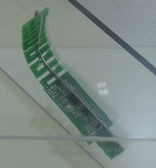
| Figure 2. Structure of bendable rigid substrate |

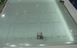
Picture 3. Bendable rigid substrate
|
As regards PCB device, Meiko Techno exhibited a unique flexible PCB. As figure 2, flexibility is obtained by inserting opening slits on the conventional rigid substrate. Especially, it's effective for flexible LED interior with some LED chips. Else, it's suitable for antenna, curved switch, and so on, too.
|


