nano tech 2019/Advanced Printing Technology Exhibition 2019/neo functional material 2019/JFex2019
Material makers announced to expand into device market of organic devices
January 30 - February 2, nano tech/Advanced Printing Technology Exhibition 2019/neo functional material 2019/JFex2019 2019 were held in Tokyo Big Sight. Main topics in these exhibitions are picked up.
Nippon Shokubai announce to expand into market of OLED lighting device
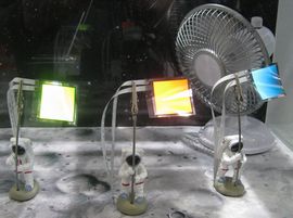
Picture 1. OLED for lighting device
|
As regards device, Nippon Shokubai demonstrated OLED lighting device effectively.
The company has proposed and developed an inverted type structure OLED
by collaboration with NHK in this field. It's composed of cathode/electron
injection layer/electron transport layer/emitting layer/hole transport
layer/hole injection layer/anode. Two original materials and layers instead
of alkali buffer material, such as LiF, Liq is adopted as an EIL. It's
composed of double layer, organic material and inorganic material. The
former is deposited by wet-coating method, on the other hand, the latter
is deposited by dry-deposition method. Its thickness is relatively thick
(10 - 20 nm). For this reason, it's easy to cover pinhole defects. And
also, atmospheric stability is superior because of non-chemical reaction
against impurity gas, such as H2O. Therefore, device can be encapsulated
by simple layer and manufacturing process, as a result, total manufacturing
process cost can be reduced. In fact, a general packing film for food can
be used as an encapsulation film. Required water vapor permeability is
10-2ü`-3g/m2/24h. As you know, that of the conventional structure OLED is approximate 10-6g/m2/24h.
In the booth, solid encapsulated device by PEN film + this encapsulation film was exhibited. Its thickness was mere 0.07 ćo. As picture 1, this sample device was flapped in the wind from a fan. And also, its quality is superior, such as, defect-free, uniform brightness, and high contrast. Furthermore, this sample was pilot-manufactured all by itself without collaboration of NHK. As you know, NHK is developing OLEDs due to realization of sheet type display, on the other hand, the company focuses only OLED lighting device, and will release OLED device until 2020. In fact, sample device can be supplied in the present moment. By the way, specification of this sample device was almost same as the conventional OLED (R,G phosphorescence, B fluorescence).
Toray appealed effective applications of organic film solar cell
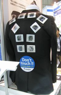
Picture 3. Generable suit |
Picture 2. Samples of organic film solar cell |
By contrast, Toray exhibited various application samples of organic film solar cell. The company announced to expand into a market of this device, too. Sample device is a bulk-hetero junction type polymer device using an original p-type material and conventional n-type material (PCBM) in light absorption layer. Its incident photon-to-current efficiency (IPCE) is 10 - 12 %. However, it can be generated in low illuminance condition, for example, 100 lux and under. It's suitable for smartphone, smart-meter, various sensors, and so on.
Furthermore, in the Riken's booth Toray exhibited a generated suit with organic film solar cell by collaboration with Riken, AOKI, and Xenoma. It's a flexible and wearable device using deposited polyparaxylene film as a substrate, and can be mounted to suit because of ultra-thin type (15 ā╩m). Device structure is same as that of the above device. As picture 3, 10 devices are mounted, total output of 280 mW is obtained. By the way, this device was mounted to suite in suit manufacturing process by heat transfer.
JEPERA developed new process technologies one after another
As concerns manufacturing process of device, Japan Advanced Printed Electronics Technology Research Association (JAPERA) indicated a project results in NEDO's booth.
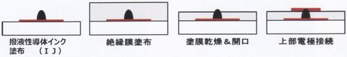 |
| Figure 1. Interlayer connection process using hydrophobic conductive ink
|
One is an interlayer connection process using hydrophobic conductive ink. As figure 1, first of all, a hydrophobic Nano size Ag ink is printed by the ink-jet printing method on the substrate. It does not almost spread on the substrate because surface of Nano size Ag grain is covered with hydrophobic protective group. In short, printing shape does not almost change with time. As a result, high contact angle of printed film can be kept. The next, insulation film is coated and dried. In this time, Ag circular cones expose with opening of insulation film selectively by thermal shrinkage. Therefore, it's possible to contact Ag circular cones and the upper electrode without photolithography process and photo mask. Its height is 3.5 - 4 ā╩m, which is sufficient for sensor devices inclusive of TFT.
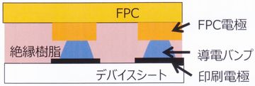 |
| Figure 2. New connection technology |
Another is a new connection process instead of ACF (Anisotropic Conductive Film) method. As figure 2, in this process, electrodes on device are connected with FPC electrodes by use of conductive bumps. A conductive Ag grain is treated by surface modification, too. First of all, ā╩m size Ag ink is coated by the dispenser, and then, insulation resin is coated on whole surface of the substrate, and finally its work is thermally bonded at low temperature, same as 100 üÄ and under. Compared to ACF method, which is necessary to bond at 180 üÄ and over, thermal damage against device and FPC is lower, and also, manufacturing cost can be reduced, too.
By the way, JAPERA will dissolve at the end of March, 2019. All printing pilot-production line (correspond to 300 ü~ 400 ćo) in Tsukuba City, Ibaraki will be alienated to AIST charge-free, and then, it will be utilized as a main system of ügFlexible IoT Consortiumüh, which will be established in near future by industry-government-academia group.
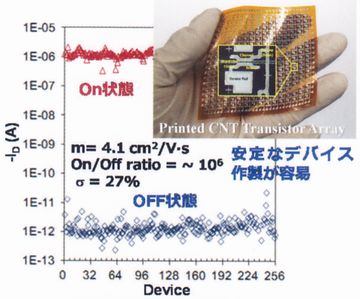 |
| Figure 3. Transfer characteristics of CNT-TFT |
ON/OFF ratio of CNT-TFT is enhanced by high purity abstraction
With respect to material, NEC appealed a CNT ink for CNT-TFT, and disclosed to license out this manufacturing technology to Meijo Nano Carbon, which is known as a Nano size carbon maker. It's an abstraction technology of semiconductor type CNT in commercial bulk CNT by making use of non-ionic surface-active agent instead of conventional ionic surface-active agent. In this technology, extreme high purity same as 99 % and over is gained.
CNT-TFT array (total 256) was pilot-manufactured by use of this CNT ink,
as a result, relative high carrier mobility same as 4.1 cm2/Vs was obtained. And also, ON/OFF current ratio was enhanced to 106 and over. In short, large problem of practical use for CNT-TFT could be
solved by this abstraction technology.
Evaporated organic film is suitable for estimation of QD material
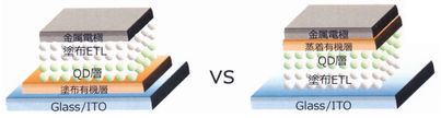 |
Figure 4. Structures of estimated device for estimation of QD material
Traditional structure (left) and New structure (right) |
As concerns estimate technology, Kyushu University proposed a new estimate method of QD (Quantum Dot) material, which is expected to be a next generation emitting material. As figure 4 - left, QD device is manufactured by making great use of wet process in general. However, it's difficult to estimate QD material exactly because of strong unstable factor by mixture phenomenon in boundary. Therefore, a new device structure (figure 4 - rightüFinverted structure) with evaporated organic film is used for estimation of QD material. As a result, it's possible to estimate QD material exactly without mixture phenomenon in boundary.
|