|
STELLA NEWS SITE is managed by Stella Corporation Inc. |

nano tech 2018 (February 14-16, 2018) |
||||||||||||||||||||
February 14-16, nano tech 2018 were held in Tokyo Big Sight. Main topics in this exhibitions are picked up. Carrier mobility of CNT-TFT is increased same as that of LTPS-TFT
As regards device, Toray exhibited CNT-TFT prototype in this year, too. Conductive assist polymer was entwined with bulk SWCNT respectively, to enhance dispersibility in liquid state, and to enhance area uniformity at film state. In this time, an original polymer instead of conventional P3HT was used as a conductive assist polymer. And also, diameter of SWCNT was optimized, such as 0.9 nm, 1.3 nm, and 1.5 nm, as a result, carrier mobility was increased from 84 cm2/Vąs (last year) to 108 cm2/Vąs. In short, career mobility of CNT-TFT is superior to that of organic-TFT and oxide-TFT, and is almost same as that of LTPS-TFT. Furthermore, ON/OFF current ratio was increased to 106 order. It became to be corresponded to display device. By the way, if diameter of CNT is thick, ON/OFF current ratio is increasedüGon the other hand, carrier mobility is decreased. In the booth, array device (100 arrays) on PET film was exhibited. Its channel length is 10 â╩m. Gate electrode, source/drain electrode, and gate insulator film were coated and patterned by the photosensitive paste method. By contrast, CNT semiconductor layer was directly patterned by the Ink-Jet printing method. Maximum process temperature was minimized to 150 üÄ. If pre-annealing treatment is adopted before main manufacturing process, it is possible to use a low thermal resistance substrate, such as PET film in this CNT-TFT. Patterning accuracy of IJ method is complimented by surface modification patterning without photo mask As concerns manufacturing system, Toray Engineering appealed an ultra-wide quasi organic-TFT sample on PEN film. This sample was produced by combination of surface modification patterning and IJ process technology. Concretely, first of all, UV light was irradiated with insulator film on PEN film at pattern shape by the mask-less DMD exposure system. As a result, UV irradiated area is changed from initial hydrophobic property to hydrophilic propertyüGon the other hand, non-irradiated area is hydrophobic still. Subsequently, ink such as Ag ink is dropped by the IJ method; as a result, ink adhered to hydrophilic area selectively. In short, high resolution and accuracy are gained by combined process. In fact, it is easy to form fine line, such as 10 â╩m and under.
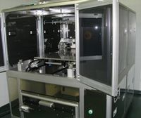
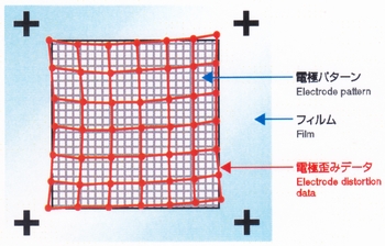
In this sample, 4 layers such as gate electrode, gate insulator film, source/drain electrode, and organic semiconductor layer were formed by the IJ method. And also, film substrate (900 ço length) was treated with respect to 600 ço length by the Roll to Roll and tact-time feeding method. By the way, this sample is manufactured by Yamagata University using Toray Engineering's system, and JSR and Future Ink prepared gate insulator material and wettable organic semiconductor material respectively. Furthermore, in this Roll to Roll type IJ patterning system (mask-less exposure unit, IJ unit, oven unit); distortion calibration process was introduced as new concept, to correspond to flexible device. As you know, in the device on film substrate, pattern distortion occurs in the annealing process due to film's essential property. In this system, first of all, fact distortion is measured, and then, initial pattern data is calibrated by reflection of measuring result automatically. Of course, this process can be introduced for mask-less process (DMD exposure system and IJ system). Thermal damage against the substrate is minimized by flash lamp annealing
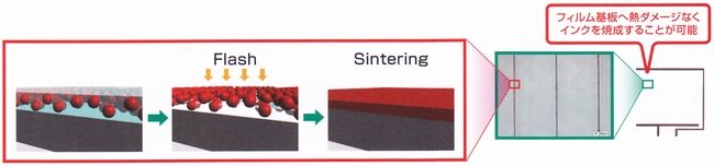
By contrast, Ushio proposed flash lamp annealing process for low thermal resistance substrate. Thermal damage against substrate and under layer can be minimized, and also, only surface of objective layer can be annealed selectively because of pulse irradiation for ultra-short time (1/1000 sec and under). Figure 2 shows process image. After sintering, single like film is gained. As you can image, in case of short pulse, irradiated depth becomes to be shallowüGon the other hand, in case of long pulse, it becomes to be deep. In this time, Nano size Cu ink (Ishihara Chemical) was annealed. After annealing, substrate was not almost damaged. Glass substrate becomes to be bendable by ultra-thinner process
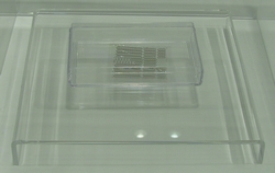
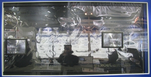
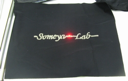
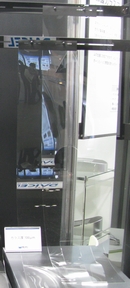
With respect to material, Micro Technology exhibited a bendable glass. Commercial glass substrate with 0.33 ço plate thickness was thinned by wet-etching treatment. In the booth, 3 samples (0.2 ço, 0.15 ço, and 0.1 ço thickness) were demonstrated. As picture 3, glass became to be bendable because of ultra-thin plate. As with the conventional glass, large size (maximum 730 ü~ 920 ço) can be supplied. The company will supply this glass with added value, in short, deposition of functional layer, patterning fabrication, hole opening fabrication, and so on. Stretchable wiring is realized by dispersion of Nano size Ag into rubber at self-aligning Japan Science and Technology Agency (JST) reported stretchable wiring as a result of ügSomeya biological harmony electronics projectüh. If fluoro-rubber, fluoro surface acting agent, and Ag flakes with â╩m size grain are mixed in synthesis process of paste, Nano size Ag is naturally generated and dispersed into rubber. Stretchable wiring is formed by making use of this phenomenon. Electric conductivity at stretched state (5 times length of initial value) is 935 S/cm, which is world greatest. It can be printed by various printing methods, such as the screen printing method. As picture 4, LED could be lighted on cloth by this printed stretchable wiring. Pigment dispersant with electrophoretic property is suitable color E-paper
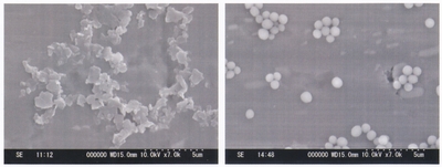
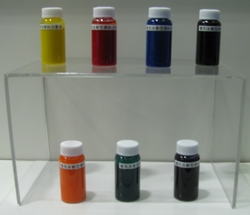
Sakata Inx introduced an original pigment dispersant with electrophoretic property for color toner and electrophoretic E-paper display. It's electrophoretic color pigment. If positive voltage or negative voltage is applied, it aggregates to negative electrode or positive electrode. As picture 5, various color types can be manufactured. In short, if it's used, color electrophoretic E-paper display can be manufactured easily. Diameter of toner can be controlled from 0.3 â╩m to 1 â╩m at will. As picture 6, this new product is just orbicular. For this reason, moving speed is increased compared to that of variant type because of easy movement property. In short, in case of using electrophoretic E-paper display, response speed is increased. Furthermore, in-plane uniformity of E-Paper is enhanced because of improvement of dispersibility. |
||||||||||||||||||||
| REMARK STELLA NEWS SITE is a free news site of FPD and PCB by Stella Corporation Inc.(This company does not release these FPD and PCB related products.) |
Novel system was released as manufacturing system of emulsion film mask. |