|
STELLA NEWS SITE is managed by Stella Corporation Inc. |

INTERNEPCON JAPAN/IC PACKAGING TECHNOLOGY EXPO/PWB EXPO/Light-Tech Expo (January 13 - 15) |
|||||||||||||||||||||
January 13 - 15, üg45th INTERNEPCON JAPAN/33rd IC PACKAGING TECHNOLOGY EXPO/17th PWB EXPO/8th Light-Tech Expoüh were held in Tokyo Big Site. As expected, technology for wearable device attracted attention. In this article, main topics are close-up.
Related on material for wearable device, Panasonic exhibited stretchable resin film, transparent conductive material, and conductive material. Resin film is an epoxy series transparent film, and it can be stretched by 2.5 times and over compared to initial value. In spite of high stretch, stress relaxation rate is 60 üō and over. Also, hysteresis does not occur by function of strong memory. Furthermore, heat-resistance is high such as decomposition temperature of 325 üÄ. Thus, it is endured against manufacturing process of flexible device sufficiently. Transparent conductive material is single-wall CNT film coated on plastic film without pattern. Its transmittance is 88 üō, and sheet resistance is 300 āČ/üĀ. However, it's impossible to pattern by any method except for the laser dry etching method. By contrast, conductive material is an original Ag paste. It can be patterned by various printing methods such as the screen printing method. Annealing temperature of printed film is low (140 üÄ), and specific resistance is 10-4 āČ/üĀ class.
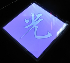
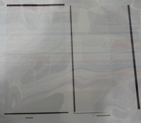
Both materials have high stretch property (10 üō and over). For this reason, if bending motion is repeated, electric characteristics is not almost degraded. Picture 1 shows a conductive Ag paste printed sample on stretchable plastic film. In the booth, the company demonstrated that it could be stretched at will by mechanical pressure from backside. Picture 2 shows microcapsule type electrophoretic display which was pilot-produced by assembly of 2 stretchable plastic films with CNT transparent electrode. The company verified that it could be operated by use of this film. By the way, the company supplies these materials, on the other hand, does not supply semifinished product such as stretchable plastic film with patterned electrode. Stretchable material can be molded after printing or coating on plane substrate. Nagase appealed a stretchable and printable transparent conductive material ügDenatronüh. It's an aquatic material of PEDOT/PSS base. It can be printed by various printing methods and coated by various coating methods. Of course, as picture 3, it can be printed and coated on curved structure. Also, after printing on plane substrate, it's possible to mold the substrate itself. Among some models, stretchable model ügSPS-800üh has relatively ordinary resistance (150 - 5000 āČ/üĀ);however, has excellent stretch property such as 200 üō and over. Thus, if it's stretched repeatedly, it is not easy to be degraded at characteristics. Ag Nano material with high adhesion by making use of new concept
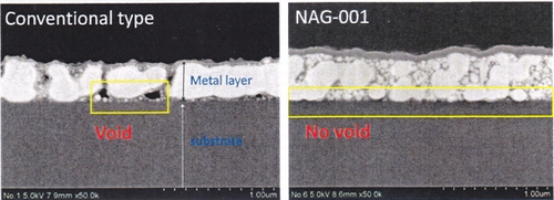
Also, the company (Nagase) introduced low temperature curing type Ag Nano size ink for flexible device inclusive of wearable device, too. In this material, not only high conductivity (10 ā╩āČźcm), but also, high adhesion against substrate are gained in low temperature annealing process. As you know, in Nano size paste and ink, Nano size powder is covered with an organic protective film respectively, in order to sure independent dispersed state. In this time, if its adhesion is too strong, after printing and annealing, organic dispersed film remains, as a result, independent dispersed state is not canceled completely, or void is generated as picture 1 (left). By contrast, in this ink, a specific thermal curing type liquid adhesion component is used as protective film, and then, after curing, it functions as adhesion layer. As a result, as picture 4 (right), void is not generated in the film. Of course, high adhesion is gained against plastic film, glass, and silicon wafer without surface treatment. Cu alloy started to be adopted at mass-production for large size touch panel
With respect to large size touch panel, Daido Steel exhibited a Cu alloy sputtering target ügSTARMESHüh for metal mesh. It's a three-way target. It's possible to deposit and pattern mesh wiring (image area) and terminal wiring (edge area) at the same time by use of STARMESH. Of course, specific resistance is 5.94 - 7.48ü~10-6 āČ/üĀ because of Cu alloy, it is nothing compared to that of ITO. Also, it's possible to control reflection rate of film by oxygen partial pressure in the sputtering deposition process, as a result, to gain low reflection ratio (minimum 10 üō). Of course, it can be wet-etched by use of conventional etchant for Cu series film. Furthermore, it's not necessary to anneal the substrate in the deposition process. It has been adopted in mass-production for large size touch panel partially. Its price is almost same as that of ITO target. Sumitomo Chemical started to mass-produce polymer OLED lighting device. In Light-Tech Expo, Sumitomo Chemical demonstrated polymer OLED lighting panels, and appealed to be mass-producing 109 ü~ 109 ćo panel (emission areaüF94 ü~ 94 ćo) as a main product. It's useful for design lighting. The price of single color type is 8,000 yen, and that of dual color type (2 colors, with picture) is 10,000 yen. Organic layers was coated and patterned by the IJ printing method, and also, in dual color type, emitting materials were patterned with respect to each area. Typical lifetime is a few dozen thousand at brightness of 70 üō compared to initial entry. However, luminance efficiency is low (2.8 - 4.6 lm/W). For this reason, the company is focusing on added value product such as design lighting. NEG produced OLED experimentally by Roll-to-Roll method using flexible glass.
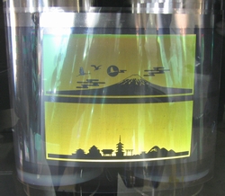
On the other hand, Nippon Electric Glass (NEG) exhibited OLED lighting panel which was pilot-produced by use of the Roll to Roll method using NEG's ultra-thin flexible roll glass ügG-Leafüh. It's world first prototype with flexible roll glass using the Roll to Roll method. By the way, prototype was pilot-produced by Fraunhofer (Germany). In the pilot-line, it's possible to correspond to substrate of width 300 ćo. Low molecule organic films and metal film were evaporated, and then, this substrate was encapsulated by a plastic film. Picture 7 shows yellow panel. In this prototype, emission was not gained on whole area because of unoptimized manufacturing process.
|
|||||||||||||||||||||
| REMARK STELLA NEWS SITE is a free news site of FPD and PCB by Stella Corporation Inc.(This company does not release these FPD and PCB related products.) |
|