|
|
STELLA NEWS SITE is managed by Stella Corporation Inc. |

|
FPD/PCB NEWS〜March 3
|
|
ROHM and Suchi Semicon Enter Strategic Partnership for Semiconductor Manufacturing in India ROHM and Suchi Semicon have entered into a strategic partnership for semiconductor manufacturing in India. The partnership aims to enhance semiconductor manufacturing capacity in India, meet growing demand in the domestic market, and eventually address global market needs. By combining ROHM’s device technologies and expertise as a global semiconductor manufacturer with Suchi Semicon’s manufacturing capabilities and operational execution strength, the two companies seek to establish a highly reliable and scalable production framework.Specifically, ROHM is considering outsourcing the back-end manufacturing processes for power devices and LSIs to Suchi Semicon and has begun technical evaluations toward mass production shipments within 2026. Through these initiatives, the companies plan to establish a robust manufacturing infrastructure in India at an early stage. In addition, both parties will share a roadmap to expand the range of package types manufactured in India, aiming to broaden their product lineup. |
|
FPD/PCB NEWS〜February 27
|
|
Seiko Epson Completes Investment in Rapidus Seiko Epson announced to complete its investment in Rapidus.Rapidus is accelerating research and development toward the mass production of cutting-edge logic semiconductors through a third-party allotment of shares centered on 32 private-sector companies. Epson decided to invest in Rapidus in order to further contribute to and collaborate with the company, recognizing that Rapidus' initiatives help strengthen the competitiveness of Japan's semiconductor industry. Epson aims to leverage its core strengths in “Sho?Sho?Sei” (efficient, compact, and precise) technologies to support these efforts. Epson has also been supporting the development of back-end semiconductor processes at Rapidus. This includes cooperating in the establishment of infrastructure for back-end development by leasing part of its Chitose Site (Chitose, Hokkaido), located adjacent to Rapidus, to “Rapidus Chiplet Solutions,” Rapidus’ R&D hub for semiconductor back-end processes. |
|
FPD/PCB NEWS〜February 25
|
|
Doshisha University and Shimadzu Conclude Comprehensive Education and Research Collaboration Agreement Doshisha University and Shimadzu Corporation have entered into a comprehensive agreement on education and research collaboration to mark the 150th anniversary of both institutions.Through industry?academia collaboration, the partnership aims to strengthen university education as well as recurrent and reskilling education, while promoting human resource development and joint research in the field of science communication. |
|
FPD/PCB NEWS〜February 17
|
|
IBIDEN Invests for High-Performance IC Package Substrates IBIDEN announced to approve a capital investment plan for its electronics business, amounting to approximately 500 billion yen over the three-year period from fiscal year 2026 to fiscal year 2028.As the first phase of this plan, the Company announces our resolution to implement additional capital investment, primarily for the existing Gama Plant (Cell6), for the purpose of expanding the production capacity of high-performance IC package substrates, mainly for high performance servers. |
|
FPD/PCB NEWS〜February 16
|
|
UBE Invests in Immaterial (U.K) UBE invested in Immaterial (United Kingdom in their top up to the A2 round capital raise. Immaterial is an early stage company aiming to commercialize CO2 capture technologies utilizing densified monolithic Metal-Organic Frameworks (m-MOFs). |
|
FPD/PCB NEWS〜February 12
|
|
Mitsubishi Electric and Indian Institute of Technology Hyderabad Sign MOU to Strengthen Industry-Academia Collaboration Mitsubishi Electric announced to sign a memorandum of understanding (MOU) with the Indian Institute of Technology Hyderabad (IITH) to promote industry academia collaboration in science and technology, effective for a three-year period until February 2029.Under the agreement, Mitsubishi Electric and the IITH will promote joint research and personnel exchanges in various scientific and technological fields, including artificial intelligence, quantum technologies and cybersecurity. By strengthening industry academia collaboration, they aim to accelerate the development of technologies and the societal implementation of research results in order to contribute to a more sustainable world and nurture talented research and development (R&D) personnel. |
|
FPD/PCB NEWS〜February 9
|
|
Konica Minolta Collaborates with Swiss Public Research Institute iPrint to Expand Applications of Inkjet Technology Konica Minolta has begun a collaboration with the Swiss public research institute iPrint to expand the range of applications for its inkjet technology.Through this collaboration with iPrint-an institute that attracts inkjet-related companies and engineers from around the world and is highly active in applied research on inkjet technologies-Konica Minolta aims to accelerate the development of new applications for inkjet technology and the identification of new collaboration partners, thereby driving further business expansion. |
|
FPD/PCB NEWS〜February 6
|
|
AIST Group Establishes “Honda R&D?AIST Diamond × Electronics Collaborative Research Laboratory” with Honda R&D and AIST AIST Group, AIST Solutions, and Honda R&D Co., Ltd. have established the “Honda R&D AIST Diamond × Electronics Collaborative Research Laboratory” at the National Institute of Advanced Industrial Science and Technology (AIST).In 2023, AIST and Honda R&D signed a joint research agreement on diamond power devices capable of handling high voltages and large currents for automotive drive applications, and successfully demonstrated ampere-class switching characteristics of diamond power devices for the first time in the world. With the establishment of this new laboratory, the partners will promote research and development leveraging diamond’s unique properties as an “ultimate” semiconductor, focusing on the development of diamond power devices for mobility applications that surpass the performance of SiC, as well as next-generation electronic devices suited to a digitalized society. Through these efforts, the laboratory aims to contribute to the application of diamond power devices to mobility, including new fields, and to the reduction of power consumption, a key societal challenge. In addition, the laboratory will serve as a hub for open innovation, bringing together ideas utilizing diamond semiconductors from related domestic institutions and fostering the creation of a collaborative ecosystem. |
|
FPD/PCB NEWS〜February 5
|
|
|
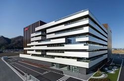
Murata Manufacturing's Production Subsidiary Fukui Murata Manufacturing Completes Ceramic Capacitor R&D Center
The five-story building has a total floor area of 41,709 square meters. The facility aims to strengthen technological capabilities in the development and manufacturing of ceramic capacitors, the company’s core business. |
|
FPD/PCB NEWS〜February 4
|
|
Mitsubishi Materials Develops Sintered Copper Bonding Materials Using Submicron Copper Particles: Copper Paste and Copper Sheet Mitsubishi Materials announced to develop sintered copper bonding materials in the form of copper paste and copper sheet using submicron copper particles that enable low-temperature sintering and bonding compared with conventional copper powders.The company developed submicron copper particles with particle sizes of 100?200 nm, extremely low levels of metallic impurities, and high sinterability enabled by a proprietary particle surface coating design. By using these particles, Mitsubishi Materials commercialized copper paste and copper sheet as copper bonding materials that offer low-temperature bonding (200?250℃), large-area applicability, and high reliability, serving as alternatives to conventional silver-based sintering materials. |