|
STELLA NEWS SITE is managed by Stella Corporation Inc. |

40th NEPCON JAPAN (Jan. 21-23, 2026)
40th NEPCON JAPAN Active Proposals for New Processes for Perovskite Solar Cells
From January 21 to 23, “NEPCON JAPAN 2025?The 40th Electronics Development and Implementation Exhibition?” was held at Tokyo Big Sight. What stood out this time were demonstrations targeting perovskite solar cells, which now seem to have been officially recognized as next-generation solar cells, with multiple new manufacturing process technologies proposed. Based on personal judgment and bias, the main topics are picked up below.
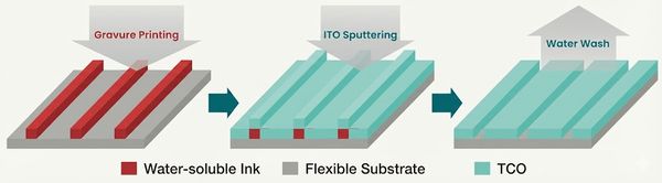
Patterning ITO Transparent Conductive Films for Perovskite Solar Cells Using Printing + Lift-Off
Artience proposed a new patterning method for ITO anodes and other layers in perovskite solar cells, called the “printing?lift-off method.” As shown in Fig. 1, a water-soluble ink is gravure-printed onto the substrate, after which a conductive film such as ITO or metal is deposited by sputtering. Then, through a water-washing process, only the conductive portions formed on top of the water-soluble ink are removed by lift-off. In processing tests, the company succeeded in patterning L&S = 65 μm / 5 mm patterns without short defects.
Fig.1 Process flow of the printing-lift-off method
Naturally, the process is applicable not only to glass but also to various plastic films with continuous roll-to-roll processing. At the booth, a wide flexible roll with patterned Al film, as shown in Photo 1, was exhibited, demonstrating compatibility with wide widths of up to 300 mm.
As can easily be imagined, the greatest feature is total cost. Compared with conventional laser etching or photo-etching methods, the company emphasized that this approach can significantly reduce costs. Specifically, a staff member commented that “based on its potential, processing could be done at about one-fifth the cost of photo-etching.” As for the business model, the basic approach is to supply printed substrates with water-soluble ink already applied, but depending on demand, the company may also supply the water-soluble ink itself. In addition to perovskite solar cells, the method is said to be effective for patterning FPCs using copper.
Pic.1 Flexible film with patterned Al film
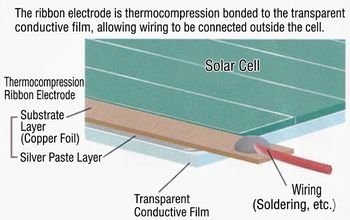
Connecting Perovskite Solar Cell Cells and Wiring Without ACF and FPC
Kaken Tech developed a conductive thermocompression-bonding ribbon electrode as a connection tool between the transparent conductive film of perovskite solar cells and wiring, proposing a new process that does not use conventional anisotropic conductive film (ACF) and FPC.
This ribbon electrode consists of a rolled copper foil base layer laminated with a silver paste layer, and is available in both reel and strip formats. As shown in Fig. 2, it is thermocompression-bonded onto the transparent conductive film of the perovskite solar cell, with wiring connected outside the cell. Thermocompression bonding can be performed at a low temperature of 100-120℃ for a short time of 60-120 seconds, making it applicable to low heat-resistant substrates such as PET films. As mentioned above, unlike processes using ACF, there is no need to use FPCs, which is overwhelmingly advantageous in terms of cost. In principle, the technology could also be applied to displays such as TFT-LCDs, but because fine-pitch processing is difficult, applications are expected to be limited to perovskite solar cells for the time being.
Fig.2 Usage sample of thermocompression ribbon electrode on perovskite solar cell
Korean Manufacturer Showcases IJ Printers for Perovskite Solar Cell Manufacturing
Korean manufacturer Gosan Tech exhibited perovskite solar cells fabricated on 370 × 470 mm glass substrates and film substrates, revealing that they have already entered the sample-supply stage. At present, however, prototype capacity is only several hundred sheets per month, with plans to move toward some form of mass production in the near future.
Pic.2 Desktop type IJ printer for perovskite solar cell
At the same time, the company has commercialized inkjet (IJ) printers for perovskite solar cell manufacturing. These systems coat hole transport materials, electron transport materials, perovskite materials, and sealing resins. As shown in Photo 2, the company exhibited a desktop-type IJ printer called “Pulse Pro 50.” It also proudly highlighted that it has already commercialized a semi-mass-production system compatible with 2G size (Wave Pro 500) and a mass-production system compatible with 5G size (Beat Pro 1300).
Korean Materials Manufacturers Also Promote Materials for Perovskite Solar Cells
Meanwhile, Korean materials manufacturer UniJet promoted materials for perovskite solar cells. Specifically, its lineup includes PbO-based perovskite materials, the electron transport material SnO2, SAMs (Self-Assembled Monolayers), and polymer inks for encapsulation. Inkjet coating is recommended for all of these materials, and in a prototype tandem device, a photoelectric conversion efficiency of 22.2% was achieved.
Transferring CNT Sheets to Printed Toner to Impart Conductivity
Pic.3 Demonstration of change from insulation property to conductive propertyAmong materials for general-purpose devices, Maruai's heat-transfer CNT transparent conductive nanosheet stood out for its originality. This sheet consists of a CNT (carbon nanotube) transparent conductive film printed on a PET film with a release layer in between. For example, in the toner-type process shown in Fig. 3, after printing toner onto a substrate, this sheet is thermocompression-bonded, causing the CNT conductive layer to adhere to the top surface. As a result, toner areas that were originally insulating become conductive. In other words, electrode patterns can be formed through a simple process combining printing and thermal transfer.
Fig.3 Transfer process using toner type thermal transfer CNT film
Of course, because the sheet itself is flexible, it also offers good transfer characteristics onto curved surfaces such as containers. Photo 3 shows a demonstration in which the sheet is laminated onto printed toner to impart conductivity, clearly illustrating how easily conductivity can be achieved.


| REMARK STELLA NEWS SITE is a free news site of FPD and PCB by Stella Corporation Inc.(This company does not release these FPD and PCB related products.) |
Automatic or semi-automatic edition Various automatic calibrations such as etching calibration Customized development |
