|
STELLA NEWS SITE is managed by Stella Corporation Inc. |

nano tech 2026 (January 28 - 30, 2026) |
||||||||||||||||||||||||||||||||||||||||||
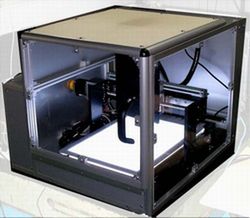
The exhibition nanotech 2026, held at Tokyo Big Sight from January 28 to 30, once again highlighted infrastructure technologies for perovskite solar cells. Demonstrations were particularly active, with major coater manufacturers showcasing dedicated system equipment. Below is a list of notable topics, selected subjectively. 1,200 mm-Wide Roll-to-Roll Coater System Dominates the BoothFirst, in the manufacturing equipment category, Hirano Tecseed, a specialized coater manufacturer, stood out prominently. The company announced the commercialization of a mass-production coater system for perovskite solar cells and exhibited a full-scale 1,200 mm-wide roll-to-roll system at one of the largest booths at the show.
The drying unit is divided into three zones. In the first two zones, hybrid heating using IR and hot-air ovens completely evaporates solvent components contained in the material. In the final zone, rapid-return drying with high-speed alternating intake and exhaust promotes perovskite crystal growth. As a result, mirror-like large-grain films are obtained. Using commercially available standard materials, prototype devices fabricated with this system achieved a power conversion efficiency of 15%. To accelerate commercialization of this mass-production equipment, the company will introduce a 200 mm-wide mass-production verification system into its test laboratory in May. Users will be able to bring their own materials for coating tests. The expected film thickness uniformity of the verification system is ±1%. Spray Coater Achieving an Astonishing 86% Material Utilization Rate
This method enables extremely uniform, high-coverage films to be deposited on substrates, including uneven surfaces. Moreover, the material utilization rate reaches an impressive 86%, an extraordinary value for spray coating. Standard film thickness uniformity of within ±5% can also be achieved. The system supports a wide range of coating liquids, from photoresists and PEDOT/PSS (poly(3,4-ethylenedioxythiophene)/polystyrene sulfonic acid) to thick solder resists, and can handle viscosities from 10 to 1,500 cps. The company manufactures and sells R&D equipment, while planning to license the technology to other coater manufacturers for mass-production systems. Solid Encapsulation of Perovskite Solar Cells Using Ultra-Thin Glass
Photo 2 shows the prototype device driving a model windmill, emphasizing its flexibility and the applicability of roll-to-roll processes in device fabrication. The water vapor transmission rate is also noteworthy, achieving a class of 10-3g/m2/day even at a glass thickness of 30 μm. GSI Creos Proposes New Materials for Organic and Perovskite Solar Cells
Although the detailed mechanism was not disclosed, as shown in Table 1, prototype devices (ITO transparent electrode / ZnO electron transport layer / PTQ-10:Y6-12 bulk heterojunction organic semiconductor layer / hole transport layer / Ag electrode) demonstrated superior performance not only compared to PEDOT:PSS-based devices but also to MoOx-based devices.
Oxide Thin Films with Extraordinary Properties Meanwhile, the National Institute for Materials Science (NIMS) announced original oxide thin films under the title “Oxide Thin Films with Conductivity Comparable to Gold, Work Function Exceeding 7 eV, and Quartz-Level Strength.”
Both materials can be deposited by sputtering using commercially available Pd-Co targets while purging with O2 gas, resulting in c-axis-oriented polycrystalline films with grain sizes of approximately 200 nm. The surface smoothness is also excellent, with an RMS roughness of 0.4 nm. In addition, both visible and near-infrared light transmittance exceed 80%. Photo 4 shows a disclosed small deposition sample; due to its thickness of 30 nm, it appears slightly brownish, but it becomes nearly transparent at thicknesses of several nanometers. A remaining challenge is the high deposition temperature of 700°C. At lower temperatures, amorphous or low-crystallinity polycrystalline films are formed. For applications requiring patterning, such as electrodes, the high corrosion resistance necessitates dry etching methods such as reactive ion etching. Display System Appearing on Wood-Grain Walls
The system consists of a signage display such as an OLED or TFT-LCD, an acrylic sheet, and a decorative ink layer, with the decorative ink providing the surface design. TOPPAN offers monitor systems in 43-inch, 50-inch, and 55-inch sizes. Even the 55-inch model is priced at 2 million yen, which seems relatively reasonable for an original interior element combined with a display. |
||||||||||||||||||||||||||||||||||||||||||


| REMARK STELLA NEWS SITE is a free news site of FPD and PCB by Stella Corporation Inc.(This company does not release these FPD and PCB related products.) |
|