|
STELLA NEWS SITE is managed by Stella Corporation Inc. |

nano tech 2022/Advanced Printing Technology Exhibition 2022/neo functional material 2022 (Jan 26 - 28, 2022) |
||||||||||||||||||||||||||||||
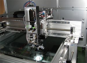
January 26-28, 2022, nano tech 2022/Advanced Printing Technology Exhibition 2022/neo functional material 2022 were held in Tokyo Big Sight. Main topics in these exhibitions are picked up. Toray improves perfection level of an original CNT-TFTsConcerns as electric devices, Toray Industries demonstrated an original CNT-TFTs in this year, too, and appealed to improve its perfection level. Conductive assist polymer was entwined with bulk SWCNT respectively, to enhance dispersibility in liquid state, and to enhance area uniformity at film state. CNT semiconductor layer was patterned at 10 É m channel length by original ink-jet printing method, was developed by Toray Engineering. Maximum process temperature was minimized to 150 Åé. For this reason, it's possible to correspond to low heat resistance substrate, such as plastic films.
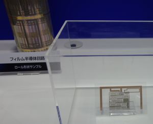
In the booth, a flexible CNT-TFT on PET film, and roll type CTN-TFT, which was manufactured by Roll to Roll process mainly. And also, as the latest press release, the company announced to fabricate radio-frequency identifiers (RFIDs) and sensors on general-purpose films and has demonstrated their wireless operations. By the way, the company produces CNT-TFT device at the moment. If market need is increased in a way, the company will examine to collaborate with other makers about manufacturing framework in near future. Highly dense Ag film is obtained by use of fine Ag grain as sinter aid With respect to materials, Osaka Soda proposed an original fine Ag grain as a sinter aid. Its diameter is 50-100nm. In short, it's situated to middle of Nano size Ag and É m size Ag. In this proposal, highly dense Ag film is obtained by use of mixed ink, which is mix of this fine Ag grain and É m size Ag.
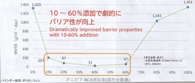
Of course, sintering temperature is lowered from 250Åé to 200Åé. However, this effect of lowering temperature is less than that of Nano size Ag grain. In short, it's suitable for not plastic films, but rigid substrate such as glass, partially, use of necessity of highly durable wiring. Clay based gas barrier material appears
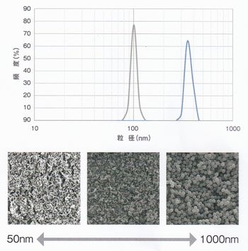
Figure 1 shows permeability of H2O. If this material is doped into the paste at 10-60% ratio, gas barrier property is drastically enhanced. This is reason why penetration path of gas is blocked by stack of montmorillonite crystal (300-500nm Å~ t=1nm). Its sintering temperature is relatively low same as 100Åé and under. For this reason, it's possible to correspond to low thermal resistance substrate, such as plastic film, paper, and so on. By the way, its appearance is gray. For this reason, transmittance and gas barrier property is relationship of trade-off. Mitsubishi Pencil appealed Nano size grain with highly uniform diameter
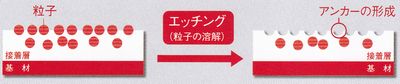
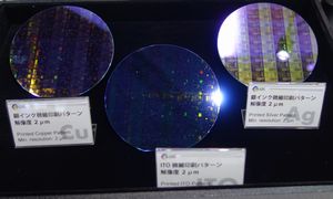
First applications are the following:á@spacer for LCD (random dispersal), áAaddition agent for film, áBporous film, áCsurface modification. In case of áC, anchor effect is formed by wet-etching using this grain as masking. In short, surface is roughly treated. Fine line same as a several É m is printed by original printing method As regards manufacturing process, National Institute of Advanced Industrial Science and Technology (AIST) appealed an originally fine printing technology, such as a few É m resolution. It is named as adhesion contrast printing. In this method, difference of adhesion of ink is skillfully applied. Concretely, first of all, laser beam is irradiated to adhesion contrast mask at pattern shape by the laser direct exposure method and etc. As a result, ink adhesion in irradiated area is increased, that in nonirradiated area keeps initial week adhesion. By contrast, an ink is coated to silicon blanket roll by the slit die coating. The next, mask roll and blanket roll are contacted, so that, unnecessary ink is transferred from blanket roll to mask roll. And then, patterned ink is transferred from blanket roll to the work substrate. As the above, ink adhesion is expressed that irradiated area ÅÑ blanket ÅÑ adhesion contrast mask. By making use of this phenomenon, ink is patterned. Tact-time of this machine is 90 sec. And also, alignment accuracy is 1 Åì and under.
|
||||||||||||||||||||||||||||||
| REMARK STELLA NEWS SITE is a free news site of FPD and PCB by Stella Corporation Inc.(This company does not release these FPD and PCB related products.) |
|