|
STELLA NEWS SITE is managed by Stella Corporation Inc. |

The 82th JSAP Autumn Meeting, 2021 (September 10 - 13) |
||||||||||||||
September 10 - 13, The 82th JSAP Autumn Meeting, 2021 was held by the online.
Topics of OLED, oxide-TFT, and perovskite solar cell are closed up based
on the proceeding.
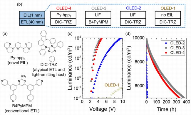
Figure 1 shows a part of the device structure of OLEDs (b), luminance-voltage characteristics of OLEDs (c), and luminance-time characteristics of OLEDs under a constant dc with an initial luminance of 10,000 cd/m2 (d). As figure 1-(c), driving voltage of OLED-3 with typical ETL and LiF was low, however, that of OLED-2 with IC-TRZ and LiF was high. On the other hand, driving voltage of OLED-4 using DIC-TRZ and Py-hpp2 was low same as that of OLED-3. And also, lifetime of OLED-4 was relatively sufficient same as that of OLED-3. As a result, if EI material with excellent electron injection property is used, it's possible to directly inject into emitting layer and also, to omit ETL. Hole injection characteristic is enhanced by utilization of surface roughness in plated Au anode
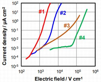
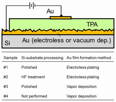
In this experiment, Au film was deposited by the electroless plating method. And then, a device was pilot-produced. It's composed of silicon substrate/Au/triphenylamine (TPA)/Au. Concretely, the substrate was treated by polishing or HF treatment, and then, Au film was deposited by the electroless plating method using electroless plating liquid include of Na(AuCl4)・2H2O, Na2SO3, Na2S2O3・5H2O, NH4Cl, and HF. The next, TPA film was spin-coated by use of 50 wt% TPA liquid. Finally, Au electrode was evaporated. Furthermore, a reference with evaporated Au electrode instead of electroless plated Au was pilot-manufactured. Figure 2 shows schematic cross-section of the layered device. As figure 3, J-E characteristic was superior in this order of sample #1>#2>#3>#4. In this time, average surface roughness (Ra) of Au electrode was rough in above order. In short, surface roughness of Au electrode is high, hole injection characteristic is increased. Dielectric/Metal/Dielectric is used as a transparent electrode of flexible OLEDs Toyama University proposed dielectric/metal/dielectric (DMD) was utilized as a transparent electrode of flexible OLEDs instead of ITO electrode. If this electrode is used, it's effective for not only flexibility, but also enhancement of characteristics. In this experiment, P(VDF/TrFE) was spin-coated on the glass as a flexible substrate. Subsequently, PEDOT:PSS was spin-coated, and then, Au film was deposited by the sputtering method. As a result, DMD electrode (PEDOT:PSS/Au/PEDOT:PSS) was completed. The next, α-NPD and rubrene were co-evaporated at mol ratio 95:5, and then, Alq3, LiF, and Al were evaporated continuously. 2 reference devices with MoO3/Au/MoO3 or ITO electrode were pilot-produced on the glass substrate due to comparison of characteristics.
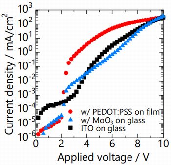
Figure 4 shows J-V curves of OLED using ITO and DMD electrodes w/PEDOT:PSS and MoO3. J-V characteristics of devices with both DMD electrodes were superior in spite of high sheet resistance compared to that of ITO electrode (9.05Ω/□). This is reason why PEDOT:PSS and MoO3 are functioning as hole injection layer because of dielectric. Figure 5 shows L-J curves of OLED. Transmittance of device with DMD electrodes was lower than that of device with ITO electrode, however, L-J characteristics of device with DMD electrodes was almost same as that of device with ITO electrode. In short, compared to both electrodes, light extraction efficiency was almost same. Upper ITO electrode can be used to organic device by relaxation of stress in deposition process National Institute of Advanced Industrial Science and Technology reported degradation of characteristics of organic devices could be avoided by relaxation of stress in ITO electrode deposition process.
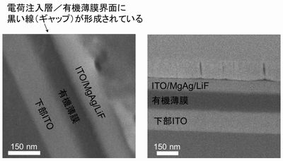
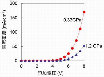
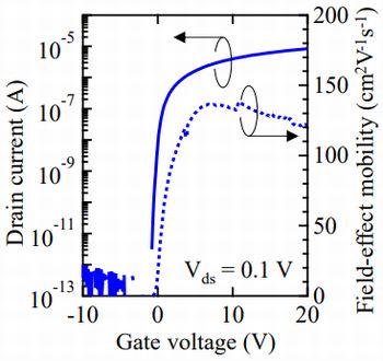
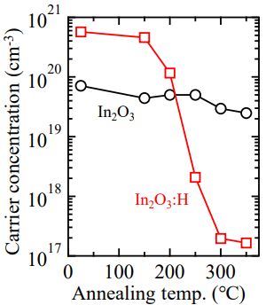
In deposition process of upper ITO electrode, H2O gas was purged into the vacuum chamber at approximate 10-4Pa due to block of poly crystallization of ITO film. As a result, ITO film became to be amorphous, and then, stress in ITO film was reduced. In proportion as reduce of stress in ITO film, as figure 6, J-V curves of device was enhanced. Picture 1 shows SEM image of 1.8GPa device and 0.37GPa device. In the former, gap in boundary of organic film and LiF was observed, on the other hand, in the latter, it's not observed. In short, device characteristics were enhanced by reduction of stress in ITO film because of suppression of gap formulation. Highest carrier mobility in oxide-TFTs was obtained by poly crystal In2O3:H-TFT As regards oxide-TFTs, the collaborative research group of Shimane University and Kochi University of Technology announced poly crystal In2O3:H-TFT with world's highest carrier mobility in oxide-TFTs. In this experiment, In2O3 film andIn2O3:H film (50nm) were deposited on the quartz substrate at Ar+O2 and Ar+O2+H2 environments by the DC magnetron sputtering method. The next, it's annealed in atmosphere at 150 - 350 ℃ for 1 hour. And then, a bottom-gate type In2O3:H-TFT was pilot-manufactured.
On the other hand, in In2O3:H film, Ne was increased to 1 digit compared to that of In2O3 film at as-deposition state, however, it was greatly reduced to approximate 200 ℃, which was starting temperature of solid phase crystallization, and it's reduced to 1.9×1017cm-3 at 300℃. In fact, after solid phase crystallization, grain size of In2O3:H was greatly enlarged to 140 nm. Furthermore, as figure 8, carrier mobility, SS, and Vth were 138.3cm2/Vs, 0.19V, and -0.2V respectively. In short, world's highest characteristics in oxide-TFTs were obtained. Perovskite film is passivated by doping trisphosphine into precursor liquid
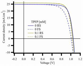
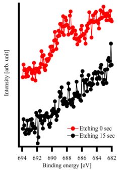
In this experiment, after SnO2 film was deposited on the substrate with FTO electrode by precipitation using chemical solution, a perovskite precursor liquid inclusive of Tris(pentafluorophenyl)phosphine (TPFP) was spin-coated, and then, it's annealed at 150℃ for 10 minutes. The next, Spiro-OMeTAD liquid was spin-coated, and then, Ag was evaporated by the vacuum evaporation method. Figure 9 shows XPS F 1s spectra of 0.1 mM TPFP-added perovskite film. Fig.10 shows J-V curves of perovskite solar cells under AM1.5 G,100 mW/cm2. In case of doping TPFP at 0.1 mM, PCEFS and PCERS were increased from 19.9% to 20.5%, and from 17.3% to 20.5% respectively because of enhancement of F.F. This is reason why device characteristics were enhanced by passivation effect of perovskite layer using TPFP. Characteristics of Sn series perovskite solar cell are enhanced by evaporation of PVK On the other hand, Kyushu University announced device characteristics of Sn series perovskite solar cell could be enhanced by depositing perovskite film using the vacuum evaporation. As you know, PCE of Sn series device is approximate 13%, which is almost half of that of Pb series device. It's difficult to deposit uniform film by the conventional spin-coating method. And also, it's easy to oxidize from Sn2+ ion to Sn4+ ion. For this reason, Sn series perovskite film was deposited by the vacuum evaporation method due to suppression of oxidation. In this time, oxygen concentration in the vacuum chamber is < 1ppb. This value is lower at 3 digit than that of N2 globe box (1ppm class), which is process environment of the spin-coating process. CsSnI3 film was co-evaporated in above low O2 concentration. And also, a sample device (ITO/PEDOT:PSS/CsSnI3/C60)/BCP/Ag) was pilot-produced.
In produced device by optimization of evaporation temperature. Jsc was greatly little. Therefore, evaporation ratio of materials was optimized, Jsc in overmuch SnI2 region was increased, and then, PCE was increased to approximate 4 times. This seems that oxidation of Sn is suppressed by non-reacted CsI and overmuch SnI2, as a result, recombination of charge in the film was decreased. However, absolute value of PCE is not sufficient. This is reason why recombination of charge occurs often by oxidation after deposition and existence of non-reacted sort. Reference 1)Inagaki, et.al.:Innovation of OLED multilayer structures using novel electron injection materials, The 82th JSAP Autumn Meeting, 2021, 11-371 (2021.9) 2)Matsuda, et.al.:Hole Injection Characteristics Using Au Electrode with Nano-Projection Structure, The 82th JSAP Autumn Meeting, 2021, 11-285 (2021.9) 3)Oku, et.al.:Fabrication of Flexible Organic Light-Emitting Diodes using Dielectric/Metal/Dielectric Electrode, The 82th JSAP Autumn Meeting, 2021, 11-382 (2021.9) 4)Suemori, et.al.:Controlling the internal stress of ITO layer for improving the performance of transparent organic light emitting diode , The 82th JSAP Autumn Meeting, 2021, 11-286 (2021.9) 5)Magari, et.al.:High-Performance Hydrogenated In2O3 Thin-film Transistors, The 82th JSAP Autumn Meeting, 2021, 16-010 (2021.9) 6)Ishikawa, et.al.:Improved Efficiency of Perovskite Solar Cells by adding fluorophenyl phosphine, The 82th JSAP Autumn Meeting, 2021, 11-066 (2021.9) 7)Takekuma, et.al.:Fabrication of lead-free perovskite solar cells with vacuum evaporation method, The 82th JSAP Autumn Meeting, 2021, 11-092 (2021.9) |
||||||||||||||
| REMARK STELLA NEWS SITE is a free news site of FPD and PCB by Stella Corporation Inc.(This company does not release these FPD and PCB related products.) |
|