|
STELLA NEWS SITE is managed by Stella Corporation Inc. |

Innovation Japan 2021 (August 23 - September 17) |
||||||||||||||||||||||||
August 23th, Innovation Japan 2021 - Online has started by the online method. Many demonstrations are disclosed until September 17th by a specific homepage. Topics for electronics device are closed up based on the homepage. Transparent oxide conductive film is formed at RT
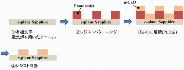
As first research result, a precursor liquid composed of dispersed Carbon Nano Tube was coated on the substrate, as a result, transparent conductive film in not only UV region, but also deep ultraviolet region was formed by UV irradiation process at R.T. Its adhesive is sufficient, and also, relatively good specific resistance same as 10-3꺐쩭m. Moreover, chemical resistance and heat resistance are sufficient. It's useful for alternative of ITO and FTO, and also, effective for electrode of solar cell and deep ultraviolet LED because of widely transparent region. In addition, pure P-type Cu2O film was formed by this method, and then, a p-n junction type solar cell with this film was pilot-produced. Besides, low resistance Cu film was formed by coating Cu precursor liquid. In this film, reflectance can be controlled by film thickness. Oxide film is patterned by the lift-off method using a-CaO sacrifice layer The research group of Kanazawa University proposed the water lift-off (WLO) process as fine patterning process of oxide thin film without etching treatment.
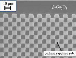
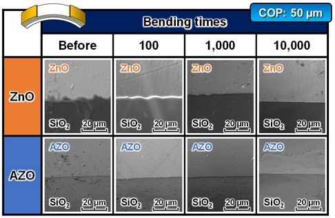
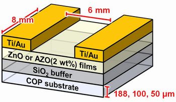
Picture 3 shows fine dot pattern same as square 7꺤m on a side. It's possible to form various structures at will without deterioration of crystallizability, surface form, and electric property. Correspond to flexible devices by stack of SiO2 buffer and ZnO semiconductor The research group of Osaka Institute of Technology appealed that oxide semiconductor succeeded to be formed on the flexible device, which was generally difficult to form oxide semiconductor because of its solid and fragility.
In this estimate, if substrate thickness was thin, deformation was decreased. Concretely, it's 188 꺤m, crack in ZnO film and AZO film was generated after 100 times curving test, and also, the substrate was broken after approximate 500 times test. On the other hand, as picture 4, at COP thickness = 50 꺤m, crack has not been observed after 10,000 times test. It's reason why if substrate thickness is thin, durability of device was improved due to decrease of deformation against SiO2 film, ZnO film, and AZO film. In fact, oxide-device with high durability (10,000 times at 5 뇇 curvature radius) has been pilot-produced. |
||||||||||||||||||||||||
| REMARK STELLA NEWS SITE is a free news site of FPD and PCB by Stella Corporation Inc.(This company does not release these FPD and PCB related products.) |
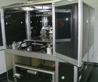
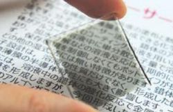
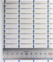
Novel system was released as manufacturing system of emulsion film mask. |