|
STELLA NEWS SITE is managed by Stella Corporation Inc. |

2021 NEPCON JAPAN 2021/35th ELECTROTEST JAPAN/22nd IC & Sensor Packaging Technology EXPO/22nd ELECTRONIC COMPONENTS & MATERIALS EXPO/PWB EXPO?22nd Printed Wiring Boards Expo/11th FINE PROCESS TECHNOLOGY EXPO/13th LED & Laser Diode Technology EXPO (January 20 - 22 , 2021) |
||||||||||||||
January 20-22, 35th INTERNEPCON JAPAN/35th ELECTROTEST JAPAN/22st IC &
Sensor Packaging Technology EXPO/22st ELECTRONIC COMPONENTS & MATERIALS
EXPO/22st Printed Wiring Boards Expo/11th FINE PROCESS TECHNOLOGY EXPO/13th
LED & Laser Diode Technology EXPO were held in Tokyo Big Site. In this
here, main topics are picked up.
Micro tech introduced a Cu2O paste, which was released by Nippon Chemical Industrial, too. As you image easily, Cu2O is oxidized in paste state yet, so that, it can be easily treated and housed. It's printed on the substrate, and then, is annealed at high temperature and blazing speed (2000 üÄ ü~ a few msec) by making use of Xe flash lamp. As a result, poly crystal Cu film is obtained by fusion of Cu grains. Of course, damage against under layer is minimized because of annealing at blazing speed. For this reason, it's possible to correspond to glass, plastic film, and paper. Specific resistance is approximate 10 ā╩āČźcm.
Patterned Al foil is used as transparent electrode of flexible device Toyo Aluminum appealed a flexible electrode substrate with patterned Al film as alternative of the conventional ITO film. It's finely patterned on Al foil by the photo-etching method. Its sheet resistance is 0.05 - 1 āČ/üĀ. This value is a few dozen parts of that of ITO film. The company can be supply this film at Roll to Roll state (maximum width üü 1100 ćo). In the booth, green OLED using this Al electrode was introduced. Curved display is gained by adoption of thinner technology of panel
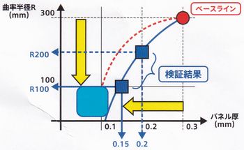
In this time, curved display was pilot-produced by use of this thinner technology. Figure 2 shows relationship of panel thickness and curvature radius. If panel thickness is 150 ā╩m, curvature radius is 100 ćo. And also, panel thickness can be reduced to 50 ā╩m at maximum. In the booth, curved TFT-LCD monitors were exhibited, but curved OLED was introduced in the literature, too. In short, it's possible to correspond to whole display module. By the way, business style is not fixed for the present moment. |
||||||||||||||
| REMARK STELLA NEWS SITE is a free news site of FPD and PCB by Stella Corporation Inc.(This company does not release these FPD and PCB related products.) |
In this system, various patterns in the substrate is captured at 1 shot by the CCD area sensor camera (50 mega-pixel), and then, AOI is treated by original image treatment technologies. AOI time of 320 ü~ 420 ćo substrate is mere 10 seconds. |