|
STELLA NEWS SITE is managed by Stella Corporation Inc. |

The 80th JSAP Autumn Meeting, 2019 (September 18 - 21) |
||||||||||||||||||||||||||||||||
September 18 - 21, The 80th JSAP Autumn Meeting, 2019 was held in Hokkaido
University. Topics of LTPS-TFT-LCD, OLED, organic-TFT, and manufacturing
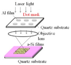
technology are closed up based on the proceeding. Variability of LTPS-TFT property is reduced by the SLA method using dot mask transfer
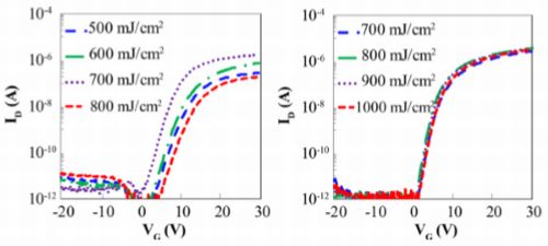
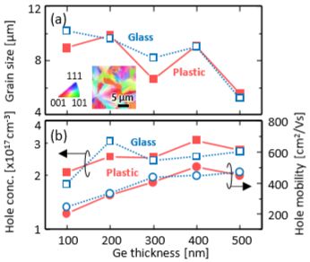
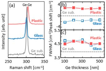
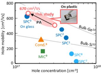
Figure 2 shows VG-ID transfers of LTPS-TFTs. TFT property of device made by dot mask transfer (b) was not easy to be influenced by laser intensity. Position and size of grain in produced device without dot mask technology are easy to be changed by laser influenceüGthe other hand, grain core in produced device with dot-mask transfer is formed at masking area and grain is melted in irradiated area, as a result, square grain is uniformly formed in the channel because of acceleration of lateral growth. In fact, variability of TFT property (N = 8) was improved from 17 % (without dot-mask transfer) to 3 % (with dot-mask transfer). In short, variability of TFT property can be greatly reduced by the dot mask transfer technology. Ge transistor emerges as a high quality flexible TFT rapidly As concerns Ge transistor, the research group of Tsukuba University and Japan Society for the Promotion of Science reported that plastic substrate device with high carrier mobility same as that of glass substrate device was obtained. In this primary experience, GeO2 film was deposited on the substrates (quartz glass and plastic film) at 50 nm thickness by the sputtering method, and amorphous Ge film was deposited at 100 - 150 nm thickness by molecular beam epitaxy method with 150 üÄ annealing. Finally, these samples were annealed in N2 environment at 375 üÄ for 150 hours due to acceleration of solid-phase growth.
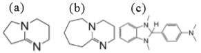
Property of inverted OLED is furthermore enhanced by EIL with a new additive The research group of University of Tokyo, NHK, Nihon Shokubai, and Oosaka University reported to enhance luminance efficiency and lifetime characteristics of the inverted OLED, which was developed using an original electron injection layer instead of conventional Alkali metal material.
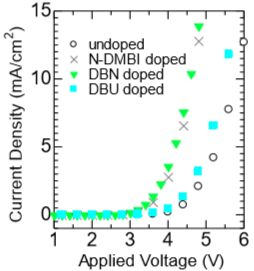
Figure 6 shows molecular structure of amidine derivative and N-DMBI. As figure 7, driving voltage of device is reduced by doping amidine derivative. And also, driving voltage of DBN device was lower than that of DBU device. As table 1, in DBN device, maximum quantum efficiency was obtained. This is reason why all injected electrons changed to emission energy by efficient electron injection from cathode. Metal halide perovskite thick film is used as carrier transporting layers of OLED
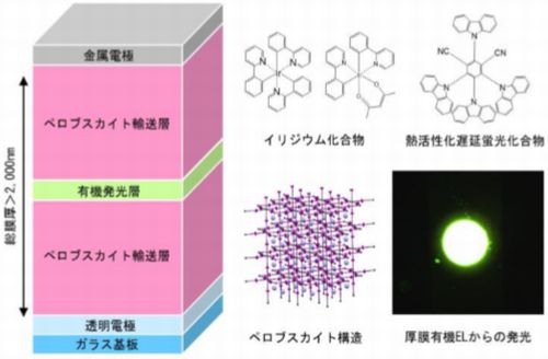
As you know, angle dependence of emission spectrum in the conventional OLED happens because light cross-talk occurs between in emission area and metal electrode. By contrast, as figure 8, light cross-talk never occurs because of insert of thick Perovskite film (1000 nm thickness) in between emitting layer and metal electrode. As a result, angle dependence of emission spectrum becomes to disappear. And also, if thickness of this Perovskite film is 2000 nm and over, high quantum efficiency same as 40 % was obtained. Furthermore, driving voltage and lifetime was practical level. Hole injection property of OTFT is improved by oxidation of Ag Nano size ink electrode
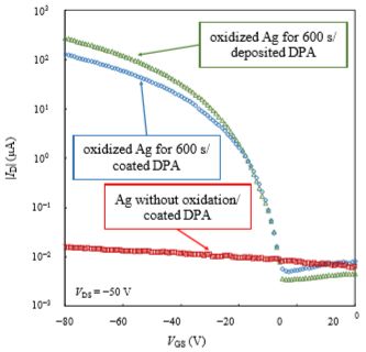
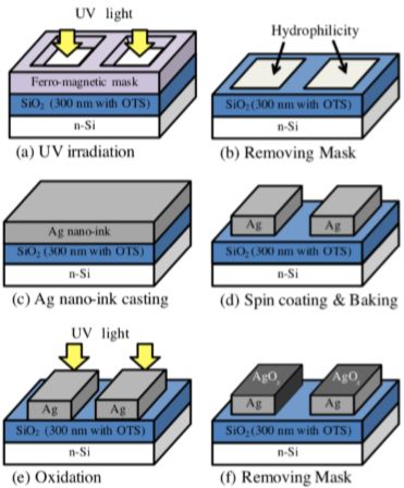
In this experience, n+ silicon wafer with OTS (octadecyl-tri-ethoxy-silane) treated SiO2 film was used as a substrate. As figure 9, Nano size Ag ink electrode was coated and patterned at the same time by surface treatment patterning process, and then, it was treated by UV light irradiation in O3 environment. The next, this sample was treated by OTS again. Finally, DPA (9,10-diphenylanthracene) liquid inclusive of chlorobenzene(C6H5Cl) solvent was spin-coated as an organic semiconductor layer. Figure 10 shows transfer characteristics of the sample. Ag/coated DPA device without oxidized treatment of Ag electrode could not operate as a transistor. On the other hand, oxidized Ag/coated DPA deice (oxidized treated for 600 seconds) could operate normally as a transistor, in common with DPA evaporated device, too. Concretely, ID and carrier mobility were 126.2 ā╩A and 0.35 cm2/Vs respectively. This is reason why hole injection property is increased because of reduction of contact resistance by oxidized treatment of Ag electrode in solution-processed device. After patterning of Cu catalyst in advance, graphene film is selectively grown National Institute of Information and Communications Technology (NICTüjreported a new patterning process of graphene film, which was a new and old Nano size material, too.
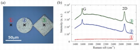
Figure 11 shows photograph of a patterned Cu thin films. (b) is Raman spectra corresponding to the position ć@ to ćB in (a). Graphene was not observed on SiO2 film from spectrum. On the other hand, peaks of 2D and G band of graphene were observed on patterned Cu film. And also, it was estimated to be not single graphene, but multi graphene. Reference 1)Imokawa, et.al.üFCharacterization of Low-temperature Poly-Si Thin-film Transistors Fabricated by Grain-Growth Controlled Selective-Laser-Annealing, The 80th JSAP Autumn Meeting, 2019, 12-027(2019.9) 2)Imajo, et.al.üFDirect synthesis of high hole mobility (670 cm2/Vs) Ge thin film on a plastic substrate, The 80th JSAP Autumn Meeting, 2019, 12-034(2019.9) 3)Suzuki, et.al.üFHighly efficient long-life inverted OLEDs by an amidine-derivative doping electron injection layer, The 80th JSAP Autumn Meeting, 2019, 11-148(2019.9) 4)Matsushima, et.al.üFThick-film organic light-emitting diodes with metal halide perovskite transport layers, The 80th JSAP Autumn Meeting, 2019, 11-217(2019.9)5)Sone, et.al.üFEffect of Oxidation Treatment on Ag Nano-ink Electrode Surface in Wet-processed OFET, The 80th JSAP Autumn Meeting, 2019, 11-564(2019.9) 6)Tominari, et.al.üFGraphene growth using patterned metal thin film, The 80th JSAP Autumn Meeting, 2019, 15-121(2019.9) |
||||||||||||||||||||||||||||||||
| REMARK STELLA NEWS SITE is a free news site of FPD and PCB by Stella Corporation Inc.(This company does not release these FPD and PCB related products.) |
|