OPEN HOUSE 2019 basic technologies for a flexible display were introduced
May 30 - June 2, OPEN HOUSE 2019 was held in NHK Science & Technology
Research Laboratories. As regards display, a few basic technologies for
a flexible display were introduced.
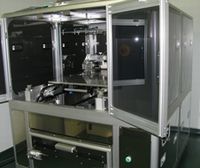
Picture 1. Solution type oxide-TFT on a plastic film |
First of all, a new manufacturing process of solution type oxide-TFT was introduced as an original technology for a flexible display. Concretely, IZO oxide semiconductor liquid was coated on the substrate by various coating methods, for example, the spin-coating method, and then, was dried. The next, deep UV light was irradiated with the substrate from opening area of a mask. As a result, irradiated area becomes to be insoluble against various etchants, such as acid because of proceeding of oxidation. Subsequently, the substrate was wet etched by making use of acid. As a result, unirradiated area is removed. In short, it's possible to form fine pattern without a photoresist and its process. In this time (Picture 1), a metal mask was used because of rough pattern, but a conventional photo mask is used for actual device. By the way, it's possible to adopt this process for other almost oxide semiconductors.
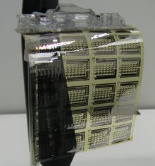
Picture 3. Pilot-produced QD device |
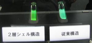
Picture 2. Comparison of UV excited emission |
On the other hand, a new quantum dot (QD) display was demonstrated by collaboration of Ulvac, too. Its QD is composed of core (ZnInP) and 2-layer shells (ZnSe +ZnS). In the past, 1 shell structure (ZnInP + ZnS) was used. By contrast, in this time, first shell was inserted. This is reason why defects are reduced inside QD. As a result, half maximum full-width of Green QD was greatly narrowed from 61 nm to 41 nm. For this reason, pure green emission (neighborhood 520 nm) was obtained. However, quantum efficiency was reduced from 3 % to approximate 1 %.
Picture 2 shows a pilot-produced device. Its structure is almost same as that of OLED except for emission layer. By the way, emission color is controlled by diameter of QD (R = 5nm, G = 3 nm, and B = 1-2 nm).
ITZO-TFT is proposed as a next-generation imaging device
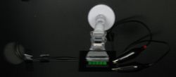
Picture 4. Pilot-produced imaging device |
Also, a new oxide-TFT was produced for a next generation imaging device. Compared to the past device, ITZO (In-Sn-Zn-O) is used as an oxide semiconductor instead of IGZO (In-Ga-Zn-O), and the back-channel structure is adopted as TFT structure instead of the etching stopper type with etching protection layer. As a result, it's easy to pattern finely because of without etching protection layer. Of course, PEP times is reduced from 6 times to 5 times. As you image easily, this is reason why chemical stability of ITZO is superior to that of IGZO. In fact, it is not damaged in source/drain manufacturing process. Of course, its film can be deposited by the conventional sputtering method using a commercial target, and also, post annealing temperature is same as that of IGZO film, such as approximate 300 ℃.
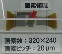
Picture 4 shows a pilot-produced device (320×240 pixels, channel length
= 2 μm). Carrier mobility and ON/OFF current ratio were sufficient for
practical use, such as 23 cm2/Vs and 108 respectively. By the way, resistance characteristic of bias stress was
not estimated yet. |