|
STELLA NEWS SITE is managed by Stella Corporation Inc. |

Innovation Japan 2018 (August 30-31, 2018) |
|||||||||
August 30-31, Innovation Japan 2018 were held in Tokyo Big Sight. New topics of manufacturing process in this exhibition are picked up. First of all, as regards printable manufacturing process, National Institute
for Materials Science (NIMS) appealed an original printable wiring circuit
technology in the booth of New Energy and Industrial Technology Development
Organization (NEDO). Fine wiring circuit can be formed without annealing
process by making use of this technology, as a result, it can be applied
to low thermal resistivity substrate such as plastic film, paper, flower
and so on.
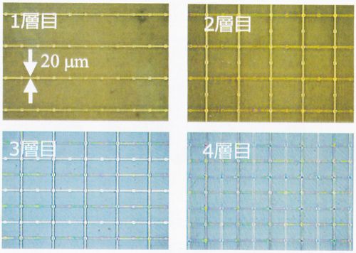
As above, fine pattern can be formed easily by use of this ink. Concretely, first of all, a hydrophobic polymer is coated on the substrate, and then, it is exposed by irradiation of UV light, as a result, irradiated area only is changed from hydrophobic property to hydrophilic property. The next, the Nano size metal ink is coated without pattern by various coating method, for example, the spin coating method. As a result, it gathers in hydrophilic area only selectively. In short, fine pattern is formed by making use of surface treatment technology. Fine line such as 1 μm width can be formed by use of this technology. In the booth, 4-layer stacking sample was introduced for effective application. AZO transparent film is deposited by new FTS sputtering method
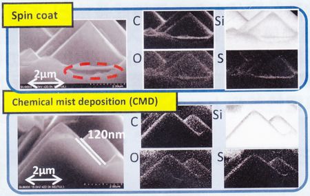
The research group have mainly researched and developed AZO film as candidate transparent conductive film of ITO film. Transmittance is 80 % and over, and specific resistance is 10-4Ω・cm in room temperature process. In the booth, AZO film on the PC film was exhibited. New spray deposition method appeared on the scene for concavity and convexity plane
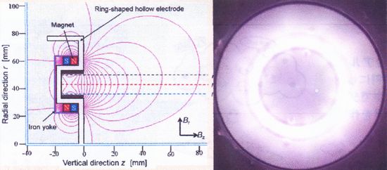
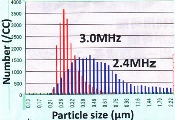
As figure 3, mist grain size can be controlled by applied frequency, and it can be decreased to minimum 20 - 30 nm. For this reason, it is effective for substrates with concavity and convexity plane, which is difficult to deposit uniformly. The research group introduced a deposited sample on silicon wafer with texture structure as an antireflection film. As picture 2, they demonstrated that it could be deposited at high uniform quality against slant plane. |
|||||||||
| REMARK STELLA NEWS SITE is a free news site of FPD and PCB by Stella Corporation Inc.(This company does not release these FPD and PCB related products.) |
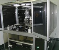
Novel system was released as manufacturing system of emulsion film mask. |