STELLA NEWS SITE is managed by Stella Corporation Inc.

Technical Report of The Institute of Image Information and Television Engineers-Information Display- (July 30)


Technical Report of The Institute of Image Information and Television Engineers-Information Display-
New technologies of flexible oxide-TFTs with polyimide substrate were reported

Technical Report of The Institute of Image Information and Television Engineers-Information Display- was held in Tokyo at July 30, 2018. In this here, two technical reports (JOLED and Japan Display) about flexible oxide-TFTs are picked up.

Reliability of PI-based oxide-TFTs is enhanced by use of PI with high volume resistivity

Mr.Tanaka (JOLED) reported reliability of flexible oxide-TFTs using transparent polyimide (PI) film in this presentation.


Fig.1 Structure of sample TFTs1)

In this research, a top-gate IZGO-TFT was used as an active-matrix array. As figure 1, 3 samples were pilot-produced. Device A is a reference (glass substrate), device B is a flexible TFT with PI substrate, and device C is basically device B, but a shield layer is inserted in the undercoat layer due to keeping a certain electric potential.

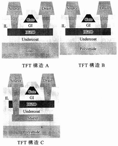
Manufacturing process is basically common;‡@Undercoat layer is formed by PE-CVD deposition of SiO/SiN films, ‡AIGZO channel is formed by the sputtering deposition and photolithography, ‡BGate insulator layer is formed by PE-CVD deposition of SiO film, ‡CGate electrode is formed by the sputtering deposition of Al film and photolithography, ‡DSource/drain region is formed in IGZO area by the sputtering deposition of AlO film, ‡EInterlayer insulator film is deposited by coating of organic film, ‡FSource/drain electrodes are formed by the sputtering deposition of metal film and photolithography.

Device A
Device B Device C 
Vth(V)
-0.32
 -0.04  -0.02
Carrier mobility (cm2/Vs)
11.6
 12.7  10.6
Sfactor (V/dec)
0.33
 0.27  0.53

Tab.1 Characteristics of sample TFTs1)

Relating to manufacturing process of device B and C, first of all, polyimide film is coated on the glass substrate, and then, annealed. The next, IGZO-TFT is manufactured on the PI film by above process flow. Finally, excimer laser is irradiated with the glass substrate from the reverse side, as a result, IGZO-TFT with PI substrate is released from the glass substrate by sublimation of partial PI layer.

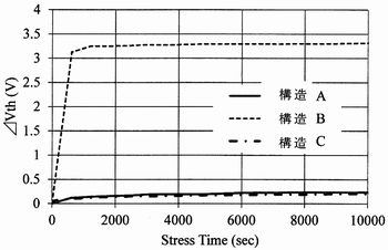
Table 1 shows device characteristics. Vth of these devices are almost same. However, carrier mobility and S factor of device C are relatively low and large respectively.
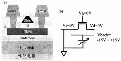
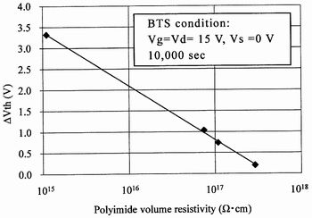
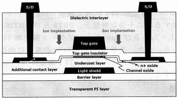
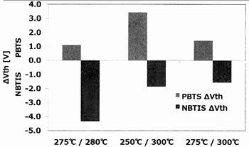
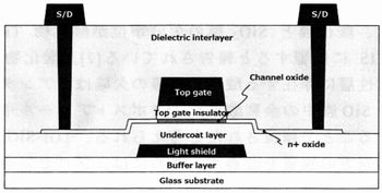

Fig.3 Cross-section structure of TFT (a) and image of PI BTS (b))1)


Fig.2 Comparison of ĢVth1)

Figure 2 shows result of BTS (Bias Temperature Stress) test. This test was done in N2 environment at 50 Ž. After 10000 sec of applied voltage, ƒ¢vth of device A and C were 0.23 V, 0.21 V respectively; on the other hand, that of device B was 3.3 V. This is reason why PI exists in IGZO-TFT. By contrast, in device C with same PI substrate, high reliability was obtained.


Fig.4 Relationship of volume resistivity of PI and ĢVth1)

To investigate this difference, the research group has run PI BTS test (figure 3). As a result, generated charge in PI film or boundary of PI film and undercoat layer changes Vth mainly. In short, degradation of boundary of channel and undercoat layer does not greatly change Vth.

And, ƒ¢Vth of device was different to correspond with kind of PI material. Figure 4 shows relationship of the volume resistivity of PI and ƒ¢Vth. If the volume resistivity of PI is high, ƒ¢Vth is low, as a result, device reliability is enhanced. As figure 4, if PI with 3~1017 ƒ¶¥cm and over the volume resistivity is used, ƒ¢Vth of TFT can be suppressed same as that of device A.

PBTS and NBTIS are related on GI deposition temperature, post-annealing temperature respectively

Mr.Yamaguchi reported top-gate oxide-TFTs for sheet type LCD.

Figure 5 shows structure of pilot-produced device. First of all, a transparent polyimide (PI) film was coated on the 4.5 generation mother glass substrate. Finally, oxide-TFT with PI substrate was released from the original glass substrate by irradiation of excimer laser.


Fig.5 Structure of top-gate oxide-TFTs2)

Concretely, first of all, SiN/SiO films are deposited on PI film as a blocking@layer by PCE-CVD method. The next, light shield layer and SiN/SiO undercoat layer are formed. Subsequently, IGZO film is deposited by the sputtering method. Also, an additional contact layer is formed area except for S/D area by the sputtering deposition of Ti film and photolithography. The next, SiO gate insulator film (TGI-SiO) is deposited at 100 nm thickness by the PE-CVD method. Subsequently, this sample is annealed in atmosphere environment for 1 hour. And also, Ti/Al films are deposited and patterned as a top gate electrode, and then, phosphorus is doped into IGZO area by ion implantation, as a result, source/drain area (n+ area) is formed in IGZO area. In short, sheet resistance of ion-implantated area is reduced as n+ area. The next, interlayer insulator film and source/drain electrode are formed. Finally, this IGZO-TFT with PI substrate is separated from the original glass substrate by the laser lift-off method. By the way, to minimize damage against PI film, process temperature is suppressed to 300 Ž and under.


Fig.6 Relationship of deposition temperature of gate insulator
and annealing temperature and ĢVth2)

Channel width and length of this IGZO-TFT are 4.5 ƒÊm and 3 ƒÊm respectively. Carrier mobility was relatively low same as 3.83 cm2/Vs, but off current was almost undetected. Also, ƒ¢Vth in BTS (Positive Bias Temperature Stress) was 1.4V, and ƒ¢Vth in NBTIS (Negative Bias Illumination Stress) was -1.56 V. These values are sufficient for driving of pixel electrode and gate driver circuit in sheet type LCD.

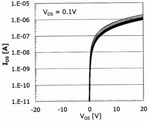
Figure 6 shows relationship of deposition and annealing temperature and reliability of IGZO-TFT. In general, if deposition temperature of gate insulator film is high, ƒ¢vth in PBTS was lowGon the other hand, if post annealing temperature is high, ƒ¢Vth in NBTIS was low.

The research group has pilot-produced a self-align type top-gate IGZO-TFT, too. Figure 7 shows cross-section structure of this sample. Unlike with the above TFT, ion implantation process and additional contact layer were detected, and gate insulator film and gate electrode were patterned at the same time by common photolithography. As a result, carrier mobility was enhanced same as 21.16 cm2/Vs. Furthermore, initial Vth (0.82 V), off current, and ĢVth in PBTS (0.39 V) were sufficient for the next generation sheet type LCD. By contrast, ĢVth in NBTIS was insufficient same as -5.28 V.


Fig.8 Ids-Vgs of self-align top-gate oxide-TFTs2)


Fig.7 Structure of self-align top-gate oxide-TFTs2)

Reference
1)Tanaka, et.al.FRequirement of a Polyimide Substrate to Achieve High Thin-film-transistor Reliability, Technical Report of The Institute of Image Information and Television Engineers-Information Display-, pp9-12 (2018.7)
2)Yamaguti, et.al.FDevelopment of Top-Gate Oxide TFTs for Plastic-Film LCDs, Technical Report of The Institute of Image Information and Television Engineers-Information Display-, pp13-16 (2018.7)


REMARK
STELLA NEWS SITE is a free news site of FPD and PCB by Stella Corporation Inc.(This company does not release these FPD and PCB related products.)

Stella's repair systemgRepair Visionh is suitable for repair use of electrode and so on. Also, it's possible to directly pattern ITO, metal, CNT (Carbon Nano Tube) films by use of this system, too.