|
STELLA NEWS SITE is managed by Stella Corporation Inc. |

The 77th Japan Society of Applied Physics (JSAP) Autumn Meeting 2016 (October 4 - 7) |
|||||||||||
September 13-16, �gThe 77th Japan Society of Applied Physics (JSAP) Autumn Meeting 2016�h was convened in Toki Messe (Niigata City). In this article, some notice oral lectures are picked up among OLED, Organic-TFT, oxide-TFT and process technology of electronics devices. Luminous voltage is raised up in OLED with FTS cathode electrode because of no increase of substrate temperature in the deposition process Tokyo polytechnic university reported research result of relationship of device property and substrate temperature in the Al cathode deposition process. In the past, research group has reported that OLED with superior luminous property was gained by suppressing incidence of high energy electron against the substrate and depositing in more than 6mTorr sputtering gas pressure in order to suppressing incidence of sputtering grain against the substrate. However, luminous voltage of this device was 8 - 10 V. In short, it's higher than that of the conventional evaporation device. To research these cause, they researched relationship of device property and substrate temperature in the Al cathode deposition process. In this experiment, first of all, ITO anode was deposited at 80 nm thickness by the FTS (Facing Target Sputtering), and then, ITO buffer layer was deposited at 0.6 nm thickness in Ar + O2 (10��) gas environment and fixed condition (60 mA, 480 V, 30 sec). The next, NPB (40 nm), Alq3 (30 nm), BCP (30 nm) and LiF (0.6 nm) are deposited continuously by the evaporation method. Subsequently, Al cathode was deposited by the FTS and the evaporation method at 50 nm thickness. As a result, OLED device was completed. When increase of substrate temperature is estimated in the deposition process, substrate temperature in the evaporation process was about 80 �� in the reverse side of the substrate. On the other hand, increase of substrate temperature in the FTS was not almost reserved. As the result of estimation of device property (voltage - current and voltage - luminous property), below points were confirmed that luminous property of the evaporation device with low temperature deposition process (less than 43 ��) is almost same as that of the FTS device, and that of the post-anneal FTS device in the vacuum condition was dramatically decreased, and it is almost same as that of the conventional evaporation device. This result indicates that different operation property of the FTS device and the evaporation device is caused by increase of substrate temperature in the deposition process. Makes Organic-TFT without the substrate by using relief reverse printed Ag gate
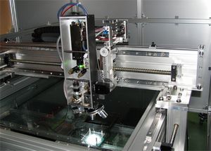
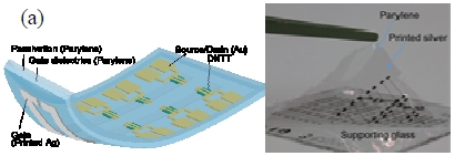
Research group of Riken, JST and Tokyo University reported Organic-TFT without the substrate by using relief reverse printed Ag gate. In this experiment, first of all, teflon (AF1600) was spin-coated on the glass substrate as release layer. The next, Nano size Ag ink (RAGT-29) was printed on the release layer by the relief reverse printing, and then, this film was burned at 180 �� for 1 hour. As a result, gate electrode was completed. Film thickness is 75 nm. Subsequently, polyparaxylylene (diX-SR) film was deposited at 300 nm thickness as gate insulator and substrate by vapor polymerization method. DNTT film was evaporated at 30 nm thickness as semiconductor layer, and then, Au film was evaporated at 50 nm thickness as source/drain electrode. Finally, polyparaxylylene was deposited on the whole layers at 300 nm thickness as encapsulation layer (figure 1-a). After release from the support substrate, thickness of the device is 755 nm.
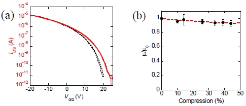
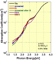
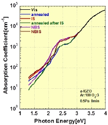
As the result of this experiment, it's confirmed that thickness of Ag electrode was possible to control from 75 nm to 500 nm by coating speed of ink in the printing process. Also, minimum thickness (75 nm) was gained while coating speed was 1 �o/sec. Furthermore, it's confirmed that this electrode could be released from teflon release layer completely, and it could be transferred to polyparaxylylene gate insulator (figure 1-b). In fact, superior transistor was realized by using this gate electrode. After release, career mobility of this device was 0.48 cm2/V�s. This value is almost same as that of reference device with evaporated Au gate electrode. Also, while stress (at 60 �� power) against vertical direction was applied, decrease of career mobility was only 4.3��. a-ITZO is advantageous to NBIS resistance properties compared to a-IGZO As you know, amorphous InGaZnO (a-IGZO)-TFT is put to practical for active matrix device of LCD. However, a-IGZO-TFT which is a typical oxide-TFT has Vth sift by negative bias illumination stress (NBIS). This problem is critical for practical use, and it has to be solved. In this time, research group of Japan University reported measure result of transistor property of a-IGZO-TFT and a-ITZO-TFT in degradation condition.
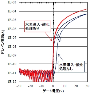
In this experiment, bottom-gate TFTs were manufactured on the non-alkali glass substrate. A-IGZO film and a-ITZO film were deposited in room temperature at 300 nm thickness by the DC magnetron sputtering method. Reflective CPM was estimated by applying some degradation conditions against these samples. Concretely, white light (1.12�~10-1W/cm) was irradiated at �|10 V, for 1 hour. Figure 3 and 4 show reflective CPM spectrum of after applied stress and post-anneal. As a result, light absorption coefficiency of a-IGZO in 1.5 eV and 2.4 eV increased greatly by NBIS. On the other hand, that of a-ITZO in same range did not almost increase. As you know, level in around 1.5 eV affects on reliability of TFT greatly. Thus, compared to a-IGZO, a-ITZO has advantageous to reliability in NIBS. Improve characteristic of wettable IGZO-TFT by hydrogen injection and oxidation process NHK reported wettable IGZO-TFT by adopting hydrogen injection and oxidation process, in order to lower annealing temperature.
First of all, In(NO3)3�xH2O, Ga(NO3)3�xH2O and Zn(CH3COO)�2H2O were mixed at fixed ratio, and then, they are solved into water solvent. As a result, semiconductor precursor liquid was prepared. The next, this liquid was spin-coated on Si wafer with thermal oxidized SiO2 gate insulator, and then, it was burned at minimum 250 ��. Subsequently, this IGZO film was patterned at island shape by photolithography. The next, this film was oxidized by hydrogen injection and oxidation annealing process (250 ��). Finally, Mo film was deposited and patterned as source/drain by using metal mask. Figure 5 shows transfer characteristics of devices with and without hydrogen injection and oxidation process. This treatment is effective for device property in relatively low process. As a result, career mobility of device was enhanced from 1.1 cm2/V�s to 3.1 cm2/V�s, and then, hysteresis was suppressed. Also, while stability of device was estimated by applying positive bias stress and negative bias stress, this treatment was useful for suppression of vth sift in bias stress environment. It is considered that device stability is enhanced in bias stress by decrease of impurities and oxygen defect. Makes Cu grid by simple process using screen mesh AIST reported that low-cost metal Cu grid electrode was made the conventional photolithography-free by a new simple process using a screen mesh as a template. First of all, Cu film is deposited on PEN film at 1 ��m thickness by the sputtering method. Subsequently, a screen mask with 325 - 500 mesh is put on this substrate, and then, polymer water solution include PVA (0.5 wt��) is dropped on the screen mask. As a result, PVA solution is spread into Cu film by capillary phenomenon, and then, PVA film is patterned like a pattern of the screen mask in the dry process. By using this masking pattern, Cu film is etched by FeCl3 methanol liquid. As a result, Cu grid pattern is gained on PEN film in same form of pattern of the screen mask.
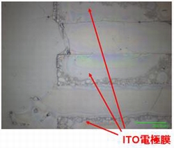
Line width of this Cu grid electrode was approximate 2.5 ��m. Its transparent ratio was more than 90 ��, and surface resistance was a dozen ��/��. PVA was covered with Cu grid electrode, so that, undercut phenomenon (side-etching) did not almost happen because of covering of PVA. Also, oxidation corrosion by hydrochloric acid gas and annealing treatment is suppressed. In short, durability is higher compared to case of without PVA. ITO film was patterned without photoresist by the mist deposition Nikon reported that ITO transparent film was patterned without photoresist by the mist-deposition (NMD) method. This is a new process by making use of phenomenon of conduct of mist, and it's possible to correspond to large substrate and Roll to Roll process easily. In this experiment, quartz is used as a substrate. First of all, fluorinated hydrophobic film is spin-coated on the substrate. The next, UV light is irradiated by use of metal mask, in order to modificate surface. As a result, UV irradiated area changes from hydrophobic property to hydrophilic property; on the other hand, non-irradiated area keeps hydrophobic property because of existence of metal mask. Subsequently, dispersion liquid with Nano size ITO is sprayed by the NMD method. In this time, dispersion liquid is atomized by using ultrasonic vibrator (2.4MHz). While dispersion liquid is water, diameter of mist is about 5 ��m. Mist is transported to the substrate by Ag career gas. As a result, as picture 2, ITO adheres to only hydrophilic area selectively; on the other hand, it does not adhere to hydrophobic area because mist conducts oneself like a droplet. In short, self-aligning process without photoresist is realized.
Reference |
|||||||||||
| REMARK STELLA NEWS SITE is a free news site of FPD and PCB by Stella Corporation Inc.(This company does not release these FPD and PCB related products.) |
|