|
STELLA NEWS SITE is managed by Stella Corporation Inc. |

Innovation Japan 2016 (August 25 - 26) |
||||||||||||
August 25 - 26, “INNOVATION JAPAN 2016” was held in Tokyo Big Sight. In this here, new topics of electronics category were picked up. Transparent electrode material with high work function (5.0 eV) is used as an anode of OLED
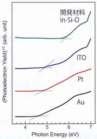
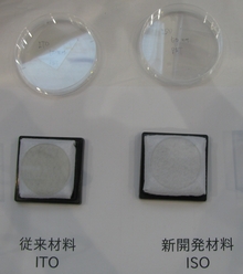
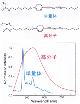
For display and lighting device of OLED, Kogakuin University has proposed an alternate material of ITO. It's In-Si-O which is SiO2 doped In2O3. In this material, high work function (more than 5.0 eV) is gained by function of SiO2. Maximum work function of this material is 6.0 eV. Furthermore, after deposition, as conventional ITO film, if this deposited film is modified by UV ozone treatment or O2 plasma treatment, its work function can be increased. As you know, if it's used as an anode of OLED, luminous efficiency of OLED is improved because of reduction of carrier injection height. Also, it's film is flat (Rms=0.2nm) because of amorphous structure, so that, it is not necessary to deposit by specific sputtering method and polish or anneal after deposition to smooth its surface. Of course, it's possible to deposit and pattern by same deposition and wet-etching process as conventional ITO. Thus, device maker does not need to develop new process and system. Furthermore, it can be deposited at room temperature. University exhibited a sample which is PET film with deposited In-Si-O film at room temperature. They demonstrated that this film was same transparent as ITO film. By the way, luminous efficiency of device is not estimated yet. White emission by single compound Ritsumeikan University announced a white emitting material which is composed of single compound for OLED. As figure 2, university synthesized polymer liquid crystal and monomer, and used Au compound which emits strongly in solid phase as a side chain. Of course, it's possible to control agglomeration state of molecule easily because of liquid crystal characteristic. Figure 3 shows its emission spectrum. As you can see, broad spectrum (x=0.3, y=0.3) is gained. External luminous efficiency is 10 - 20% because of fluorescence emission. Pure CNT film is formed burning-free by use of CNT dispersion liquid
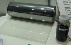
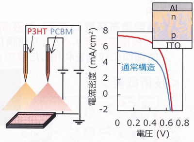
Fuji Chemical appealed a new CNT (Carbon Nano Tube) dispersion liquid for transparent electrode as result of NEDO project. Self-manufactured single wall CNT was dispersed on an original inorganic dispersion material. After coating by various wet-coating methods, user removes inorganic dispersion material by use of an original acid etchant. In short, after treatment, pure CNT film is gained burning-free. Thus, low thermal resistance substrate such as a plastic film can be used as a substrate by making use of this material. Surface resistance of this CNT film is about 300 Ω/□. This company manufactured a flexible organic film solar cell with CNT transparent anode to verify this availability, and demonstrated to able to adopt this material for organic film solar cell. However, its incident photon-to-current efficiency (IPCE) was merely 0.67 %. Device property of organic film solar cell is enhanced by use of Electrospray Deposition Saitama University appealed Electrospray Deposition method as a coating method of organic film, and reported that polymer organic film solar cell could be manufactured easily if organic layers were deposited by this method. First of all, polymer device which is composed of ITO/PEDOT:PSS/P3HT:PCBM/PCBM/Al was manufactured. P3HT:PCBM semiconductor layer was deposited by the spin-coating method; on the other hand, PCBM buffer layer was deposited by the electrospray deposition method. In this time, same solvent was used for both layers. However, under semiconductor layer was not damaged because of specification of the electrospray deposition which is medium characteristic of wet-process and dry-process.
Also, gradation layer can be deposited easily by making use of the electrospray deposition. As figure 4, it's possible to deposit gradation layer such as quasi i layer by depositing n-type material and p-type material from each other nozzle and controlling discharge time respectively. In fact, as figure 4, device property was greatly enhanced by use of the electrospray deposition. |
||||||||||||
| REMARK STELLA NEWS SITE is a free news site of FPD and PCB by Stella Corporation Inc.(This company does not release these FPD and PCB related products.) |
|