|
STELLA NEWS SITE is managed by Stella Corporation Inc. |

26th FINETECH JAPAN/7th FilmTech JAPAN/5th PLASTIC JAPAN (April 6 - 8) |
||||||||||
April 6 - 8, “26th FINETECH JAPAN/7th FilmTech JAPAN/5th PLASTIC JAPAN” was held in Tokyo Big Site. As expected, materials for flexible device inclusive of wearable device attracted attention; in particular, new materials for FPC and touch-panel were easy to notice. In this article, main topics are close-up. Ag Nano wire ink is increased a sense of presence
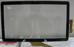
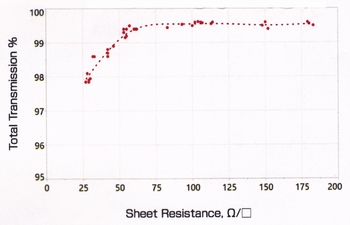
With respect to transparent electrode for flexible device use, Nagase introduced Ag Nano wire ink “Active Grid” made by C3Nano (USA). This is a transparent ink with Ag Nano wire (diameter of 37nm). It can be coated by conventional coating methods such as spin-coating, slot die-coating, and so on. Annealing temperature is 150 - 170 ℃;however, film characteristics are controlled by not annealing temperature but film thickness. Light transmittance and sheet resistance become to be trade-off relationship, however, as figure 1, transmittance is 99 % at sheet resistance of 50 Ω/□. Of course, it's effective for flexible device because of excellent flexible characteristic. And also, it can be etched by use of conventional acid series etchant in the patterning process. It's possible to supply not only ink but also transparent conductive film substrate, and to correspond to various plastic films, such as, PC film, COP film, PEN film, and COC film. As picture 1, 19.1 inch touch-panel with Active Grid was exhibited in the exhibition booth. By the way, in the past, C3Nano and Cambrios (USA) were known as Ag Nano wire maker; however, Cambrios has gone belly up. Thus, C3Nano is only Ag Nano wire maker at the moment. Stretch Ag paste appears on the scene for wearable device
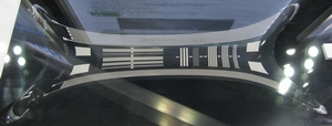
For wearable device, Asahi Chemical Research Laboratory demonstrated stretch Ag paste. In this paste, conventional μm size Ag powder and original stretchable binder are used. It's possible to correspond to various forms such as spring, stretch, fold, and twist of the substrate. However, at these conditions, initial conductance cannot be kept, but can be suppressed to increase greatly compared to conventional product in fact. Also, in the face of low temperature curing type (100 ℃), low resistance such as 10-5 Ω・cm order is gained same as high temperature curing type. As picture 2, Ag paste printed flexible substrate is exhibited at stretch condition in the booth. It's confirmed to be useful for wearable application use effectively. Invisible wiring by use of transparent polyimide film
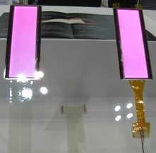
I.S.T appealed a transparent polyimide film “TORMED”. In the face of high transmittance (88 %), high thermal resistance such as Tg =300℃ is realized almost same as that of conventional polyimide film. Of course, it's possible to adopt general wet-etching process in the patterning process of wiring because of high resistance against various solvents. In the booth, OLED lighting device which was manufactured by use of FPC (this substrate base) was exhibited. As picture 3, this sample and reference OLED with conventional polyimide base FPC were exhibited in comparison. This company appealed that invisible wiring was realized. Operating ratio of etching system is increased by use of long-life etchant for IGZO With respect to related product of TFT, Kanto Chemical introduced a new etchant for oxide semiconductor. Its etching ratio is 50 nm at room temperature, in short, slightly lower than that of competing products. However, side-etching and residue don't occur almost. Furthermore, pot-life of etchant is 3 times than that of conventional product. As a result, operating ratio of etching system is greatly increased because it's difficult to remain and precipitate on the wall of etching system. It's possible to reduce total process cost accordingly.
|
||||||||||
| REMARK STELLA NEWS SITE is a free news site of FPD and PCB by Stella Corporation Inc.(This company does not release these FPD and PCB related products.) |
|