|
STELLA NEWS SITE is managed by Stella Corporation Inc. |

nano tech 2016 (January 27 - 29) |
|||||||||||||||||||||||||||||||
January 27 - 29, “nano tech 2016”was held in Tokyo Big Sight. In this here, new topics of electronics category were closed up. Firstly, with regard to device, research group of Kyushu University and Waseda University introduced a new OLED named micro fluid type OLED. It has flow channel array with a few dozen μm width which are made by the photolithography. Liquid organic emitting material is injected into flow channel. As a result, EL emission is gained in liquid part. Pyrene derivative “PLQ (Nissan Chemical)” as liquid emitting material is used. PLQ is applied for blue emission;on the other hand, rubrene doped PLQ is applied for yellow emission. These liquids are injected into flow path with stripe shape. First of all, single emissions of blue and yellow were confirmed. While these liquids were injected into flow channel each other, white emission is gained because of mechanism of additive color mixing.
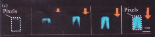
In this device, while emission intensity is reduced by time, it recovers to initial value by reinjection of liquid emitting material. Picture 1 shows emission in the case of reinjection. As you can see, emission intensity is confirmed to be recovered by time. In short, if ink (=emitting material) is replaced as the IJ printer, this device can be operated semipermanently. External quantum efficiency of device is mere 1 % or under because of large amount of light leak from edge part of flow channel. However, this is beginning value in the first device without carrier transporting layers. As conventional OLED, if these carrier transporting layers are inserted, luminance efficiency is expected to be greatly enhanced because of improvement of carrier balance.
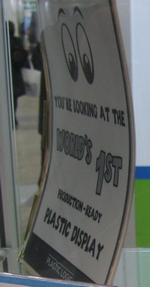
By the way, it's effective for a flexible OLED lighting device. Surely, it's advantageous for flexible device because of liquid type;however, considering flexible solid type OLED device has been in practice use, its advantage seems to be small. Plastic Logic exhibits flexible electronic paper with organic-TFT On the other hand, in the booth of Organic Electronics Saxony (Oes) which is a development project of organic device in Europe, Plastic Logic (England) exhibited a flexible microcapsule type electrophoretic display with organic-TFT. A plastic film is used as a substrate in the world's first flexible electronic paper. The company has introduced mass-production line previously. Top contact organic-TFT is manufactured by use of organic semiconductor which is dissolved in a specific solvent only
Related on material makers, Fuji Film appealed a flexible organic semiconductor device with an original organic semiconductor material. Composition of this material was not disclosed. It's dissolved in a specific solvent only. In short, while upper layer of organic semiconductor layer is patterned, inexpensive wet-etching process can be adopted by use of all solvents except for this solvent. In fact, prototype was bottom-gate top-contact type, after forming of organic semiconductor layer; source/drain electrode was formed. In this time, after patterning of source/drain, organic semiconductor was not damaged. Table 1 shows kind and characteristics of developed organic semiconductor materials. High carrier mobility such as 3 - 13 cm2/V・s is gained by using polycrystalline film deposition method such as the blade-coating. In the booth, organic-TFT with a plastic film substrate was exhibited. The company will supply these materials in near future. New material can be used instead of acrylic polymer for transparent insulation film
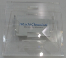
On the other hand, Hitachi Chemical introduced a new heat-resistant transparent polymer to replace conventional acrylic polymer. In the face of secret of composition, in the case of high temperature process such as 300 ℃ class, initial transmittance (90 % and over) can be kept at yellowing-free. In the booth, heat resistant transparent film substrate with this polymer was exhibited, too. However, thermal expansion coefficient of this film substrate is 70 ppm/℃ which is general value as plastic film substrate. Thus, first target is considered to be not a substrate but varnish, in short, for transparent insulator film. High conductive CNT transparent electrode is developed as substitute of ITO With respect to transparent electrode for a flexible device, AIST appealed a new CNT transparent electrode. Suspension with bulk single wall (SW) CNT and inorganic Nano grain is coated on the substrate, and then, deposited film is annealed by use of short pulse light (Xe flash tube). As a result, high conductive transparent film is gained in room temperature and atmosphere process. Its mechanism is unique. Concretely, binder in film is burned out, and added halogen compound is spread into SWCNT film by short pulse light. In short, like a doping effect is gained in this process. In the time, semiconductor CNT in bulk SWCNT changes to conductive CNT. For this reason, almost pure conductive CNT film is gained. As the result, sheet resistance of film is 60 - 70 Ω/□ at transmittance of 85 %. This value is superior to that of ITO film. By the way, it's difficult to wet-etch CNT film in general, so that, necessary to pattern by various direct printing methods or the laser dry etching method in forming process of transparent electrode. ALD-like deposition system for gas barrier film appears on the scene
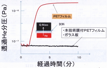
As regards manufacturing equipment, a venture company “Fhiltech” introduced unique deposition system for Al2O3 gas barrier film of OLED in the booth of Tsukuba University. It's a CVD deposition system for gradation Al2O3 film by alternate supply of TMA and H2O material gasses, but is not ALD (Atomic Layer Deposition) system. It's possible to deposit Al2O3 film at room temperature in this system. However, while thickness of 100 nm needs, long-time such as 50 minutes needs. Thus, for mass-production, batch treatment will be adopted in order to be treated some substrates at the same time. Figure 1 shows comparison of He gas permeability against PET film, glass, and PET film with Al2O3 film. As you see, gas barrier property of PET film with Al2O3 film is almost same as that of glass. Of course, it's sufficient for gas barrier film of flexible OLED because permeability of He is higher than that of water vapor and oxygen. |
|||||||||||||||||||||||||||||||
| REMARK STELLA NEWS SITE is a free news site of FPD and PCB by Stella Corporation Inc.(This company does not release these FPD and PCB related products.) |
|