|
Basic structure of OLED
■Hetero junction device
Small molecular
Fluorescence device (Standard)
Fluorescence device with hole injection layer
Fluorescence device (Alkali doped type)
Phosphorescence device
Polymer device
Fluorescence device (Standard)
Fluorescence device with interlayer
Phosphorescence device
Hybrid device of small molecular and polymer
■Homo junction device
■Structure example of long life device
Boundary-less device
Alloying device
■Multi photon mission (MPE) device
Hybrid device
■Hybrid device of OLED and organic film solar cell
■Hybrid device of PDLC, OLED, and organic film solar cell
■Mirror display
■Transparent OLED + e-paper hybrid module
3D technology
■Method to use a specific glasses
LC shutter glasses method (Time sequential method)
Polarized glasses + patterned phase difference film (Space division method)
■Specific glasses-free method
Parallax barrier method
Time sequential driving + parallax LC barrier method
Lenticular lens method
Kind and manufacturing process flow of OLED panel (general theory)
■Small molecular panel
R, G, B independent type PM-OLED
R, G, B independent type AM-OLED
CF + microcavity R, G, B independent type AM-OLED
CCM type PM-OLED
CCM type AM-OLED
CCM type AM-OLED (Inverted top emission panel)
CF type PM-OLED
CF type AM-OLED
COA type AM-OLED
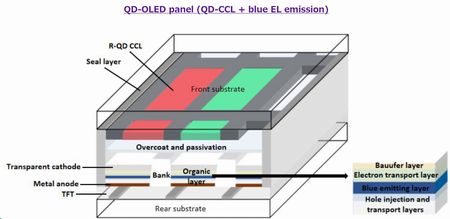
QD-OLED
■Polymer panel
R, G, B independent type PM-OLED
R, G, B independent type AM-OLED
■Assembled panel
■Single substrate panel (Thin film encapsulation)
■Single substrate panel (Solid encapsulation)
Pocess flow of OLED (particular theory)
■Forming process of transparent anode
■Forming process of bus electrode
■Forming process of insulator layer
■Forming process of cathode-separator
■Forming process of bank
■Forming process BM (black matrix)
■Forming process of CF
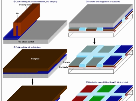
■Forming process CCM layer
■Deposition process of passivation layer
■Manufacturing process of overcoat layer
■Forming process of electron injection layer
■Forming process of small molecular emitting layer
■Forming process of blue emitting layer of CCM panel
■Forming process of white emitting layer of CCM panel and CF panel
■Forming process of polymer emitting layer
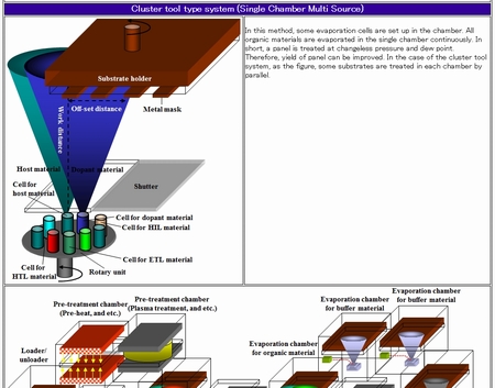
Kind of evaporation cell
■Forming process of alkali buffer layer/alkali doping layer
■Forming process of hole transporting layer
■Forming process of electron transporting layer/hole blocking layer
■Forming process of hole injection layer
■Forming process of interlayer
■Forming process of metal cathode of PM panel
■Forming process of cathode of the dual emission panel
■Forming process of co-cathode and pixel electrode (Top emission panel)
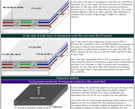
■Forming process of transparent cathode
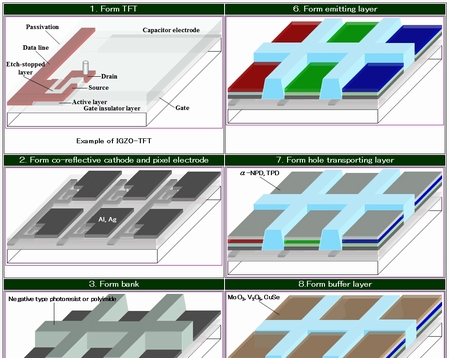
■Forming process of TFT
Manufacturing process of LTPS-TFT
Manufacturing process of IGZO-TFT
Manufacturing process of μC-Si TFT
Manufacturing process of a-Si TFT
Manufacturing process of CGS-TFT
Manufacturing process of the bottom gate/top contact structure organic TFT
Manufacturing process of the bottom gate/bottom contact type organic TFT
Manufacturing process of the top gate structure organic TFT
■Seal layer forming process
■Encapsulation process by flat glass
■Encapsulation process by cap glass
■Thin film encapsulation process of single substrate panel
■Solid encapsulation process of single substrate panel
■Scribe and break process
■Making panel thinner process
■A word of caution in manufacturing of OLED with flexible substrate
Case of using flexible substrate with film shape
OLED is manufactured on original substrate, and then transferred to plastic filmResin is coated on support substrate and cured, and then, TFT and OLED are manufactured on resin film, finally, support substrate is released (The resin film is used as substrate) |