STELLA NEWS SITE is managed by Stella Corporation Inc.
STELLA NEWS SITE is managed by Stella Corporation Inc. |
|
Manufacturing process of LTPS-TFT-LCD 2025 edition |
|
|
Explain LTPS (Low temperature poly-Si) TFT-LCD Manufacturing process by illustration Explain TFT structure, and process flow of TFT array, CF array, LC cell, and module assemble. Easy to look at the file using any PC because of the format of browser, for example IE (Internet Explorer) |
|
CONTENT |
||
|
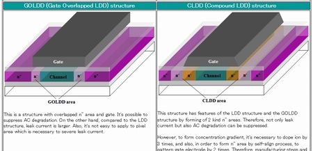
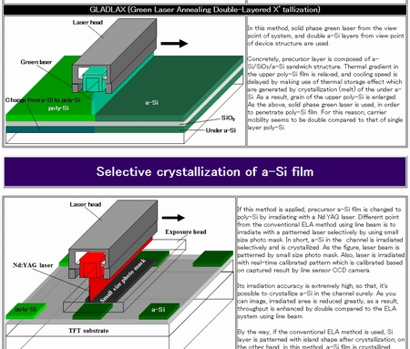
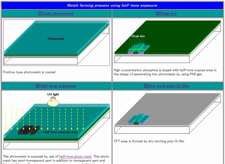
üĪStructure of LTPS-TFT-LCD üĪCrystallization process üĪTFT array process üĪCF (Color filter) forming process üĪLC cell process üĪModule assemble process üĪLiquid crystal material and display mechanism üĪStructure of backlight module üĪ3D technology Specific glasses-free method Detail of material and system is explained |
|
|
|
Full-original CD-ROM |
||
|
CD-ROM for Windows üĢ Macintosh
PriceüF23,000 yen (free shipping) Release dateüFMay 12, 2025 1-1544-7 Kaijincho Minami, Funabashi, Chiba, Japan Zip: 273-0024 Tel: +81-(0)47-432-5031 Fax: +81-(0)47-432-5032 e-Mail support@stellacorp.co.jp https://www.stellacorp.co.jp
|