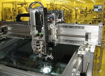
Revolutionary laser repair system “Repair Vision”
It supports dry-etching directly in addition to repair
▲AI image
■It equips ultra-high accuracy and high speed motion controller by micro-step control with less than 0.1 μm, Nd:YAG Q switch laser (2nd harmonic:532nm) which is stable and processes cut part of physical object sharply. By the way, it can equip other laser beam head, too. It's possible to not only eliminate short defect with line shape but also trim away shape defect such as fine indefinite shape without any change and eliminate its defect because it can irradiate with a laser beam with line shape.
■It can eliminate open defect of Cr, ITO, Au, Cu and so on. You can use this machine not only as repair system but also laser dry etching system that etches whole surface directly by dry-etching because you can etch open defect and form fine pattern such as minimum L&S=2μm.
▲Process flow
■Operator can repair while seeing physical object on device substrate by
monitor because this machine equips a CCD camera (USB) with a lamp.
■It operates by use of our CAD/CAM system “Stella Vision for Java”. It equips GUI with user-friendly, so that, it's possible to operate easily for anyone. Communication form is a serial interface. It supports multiple platforms because of using Java as programming language.
■It has control function of accelerating rate and XY alignment function, so that, users can ensure traceability.
■It can capture high resolution and high quality image because of use of CCD camera (USB2.0 standard).
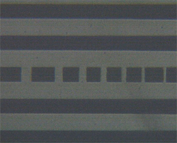
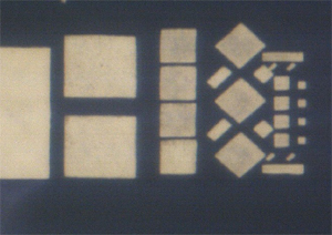
▲Picture of laser repair of Cr pattern
(line width=10 μm)
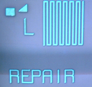
▲Picture of laser etching of ITO pattern
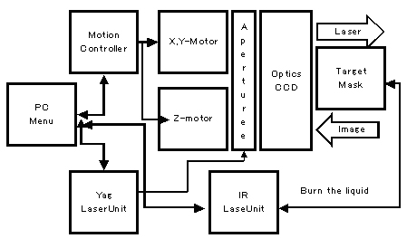
▲System diagram
Figure 1 Comparison of patterning flows
Let's see practical repair work and laser dry-etching work. First of all, you configure process condition such as energy density of a laser. Subsequently, you condescend on area of repair work and laser dry-etching on PC monitor. In this case, you can draw any shapes at will easily by mouse operation. In short, you can draw a lot of shapes by use of the template such as circle shape, line shape, and so on. Following these, you try to repair. You can confirm a result of repair immediately on PC monitor. Also, you can measure dimension of repair area, too.
Picture 2 shows appearance of repair of Cr film (100nm thickness) in hard chrome photo-mask. You can confirm it's possible to repair based on setting shape at will.
Picture 3 shows an experiment sample of direct dry-etching for use. In this case, minimum line width is about 2 μm. It is expected to be possible to draw up fine pattern such as L=1 μm by optimization of process condition.
This direct dry-etching is effective for R&D use. As you know, it's possible to dry-etch an object based on design data directly, so that, to reduce process steps drastically compared to the conventional photolithography and direct laser plot + photolithography which draws up photo-resist pattern by laser plot. You can manufacture a sample device easily and speedy.
Picture 1 Setting up of repair shape
Picture 2 after repaired
Picture 3 Experimental sample of direct patterning(line width=minimum 2 μm)
It is effective for the below use applications
◆Repair of short defect use
Repair of photo-mask with high accuracy
Repair of ITO electrode in STN-LCD, PM-OLED
Repair of various electrodes in TFT-LCD (supports Gen.5 glass substrate)
◆Direct laser dry-etching use
This system makes it possible to form fine pattern such as L&S=2μm
Fine patterning for R&D use
Manufacturing MEMS, MCM, and etc. use
Basic layout of this system
PC controller
operates by Windows machine, and controls stage & a laser beam.
Motion controller
controls XY motion and speed.
Optics
equips high precision Plan-Optics. It's a VAPE unit which focuses on the target based on defect size with accuracy.
Laser
266 nm or 532 nm Q switch Nd:YAG laser for short defect use
80 nm 1 W IR laser(optional) for baking of the paste(for open defect use
CCD camera
observe all processes by a CCD camera(to protect operator’s eye)
It has capture function for a report of the result, too.
Correct of open defect(optional)
Au or Pd paste
Cleaning in N2 environment(for lens cleaning in correct process of short defect
coordinate movement(absolute, relative), speed control, setting of alignment, reading of outside file(coordinate data), others
■Others
Main optional function
measurement software, specific shape aperture
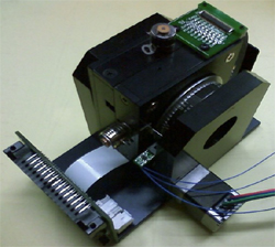
▲Next Gen. Laser repair head
▲Specific component of optics
Stella manufactures specific components for laser repair system by ourselves. Each other component equips a microcomputer and controls multiple channels at the same time by communication from main unit. Therefore, it's possible to correspond to aging variation real-time and to operate in stable by precision control of the latest optical components which are compose of high-end optical components.
Our element technology is absolutely imperative technology to follow-up the next generation technology revolution real-time. It's possible to upgrade at all times. Therefore, our technology will be enhanced compared to that of competitive company in the near future.
For example, the next generation repair head (right picture) developed by ourselves is compose of laser head, optical device and remote control system, opto-mechatronics component, mini servo unit, motion controller, image processing board, software of image processing space filter, control software, data processing software, CAM system.
These components are manufactured by ourselves. For this reason, there is no black box in all components.