|
STELLA NEWS SITE is managed by Stella Corporation Inc. |

The 68th Japan Society of Applied Physics (JSAP) Spring Meeting 2021 (March 16-19) |
||||||
March 16 - 19, The 68th Japan Society of Applied Physics (JSAP) Spring
Meeting 2021 was held by online method. Topics of oxide-TFT, organic-TFT,
and organic film solar cell are closed up based on the proceeding.
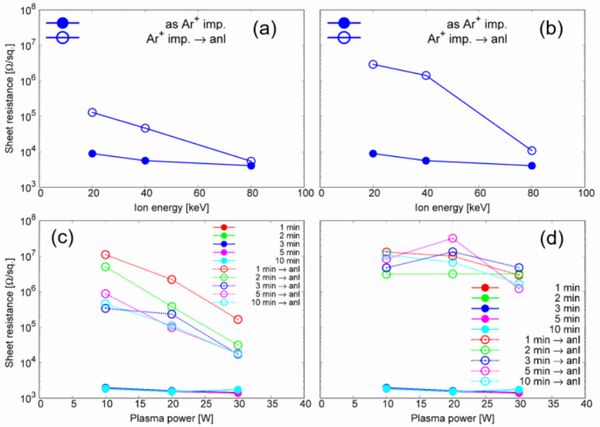
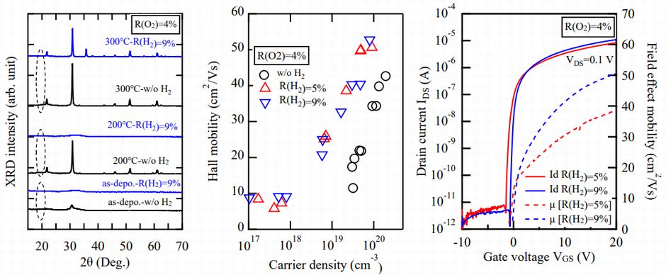
In this experiment, first of all, a-IGZO film was deposited at 50 nm thickness on the glass substrate (EAGLE XG) by the ICP sputtering method using InGaZnO4 target. Process condition is the following; �@gas flow�FAr/O = 95/5 sccm, �Apressure�F0.9 Pa, �BRF power�F7 kW, �Cvoltage�F�|400V. Ar+ ion was implanted at 1 �~ 1015 cm-2, 20 - 80 keV due to reduction of resistance. On the other hand, Ar plasma was irradiated at 20Pa, 10 - 30 W for 1 - 10 minutes as reference, which was the existing technology. These samples were annealed at 250 �� and 300 �� in atmosphere. And then, their sheet resistances were estimated before and after anneal. Figure 1 - (a) shows relationship of sheet resistance of a-IGZO film and ion energy after Ar+ ion implantation and 250 �� anneal. After ion implantation, sheet resistance was reduced to 3 �~ 103 - 104 ��/��. By contrast, after ion implantation at 20 keV, 40keV and 250 �� anneal, it was increased to 104 - 105 ��/��, however, in case of 80 keV, it was kept at as implantation. Furthermore, as figure 1 - (b), after Ar+ ion implantation at 20 keV, 40 keV and 300 �� anneal, it was increased to 106 ��/��, on the other hand, in case of 80 keV, it was 104 ��/��. Figure 1 - (c) shows relationship of sheet resistance of a-IGZO film and plasma power after Ar plasma irradiation and 250�� anneal. After plasma irradiation, sheet resistance was reduced to 103 ��/�� regardless of irradiated energy and time, on the other hand, in case of 300 �� anneal, it was increased to 106 -108 ��/�� further. Above result means that in case of plasma irradiation, oxygen defect (Vo) is reduced by O2 and H2O in atmosphere because Vo is generated in surface neighborhood of a-IZGO film�Gon the other hand, in case of ion implantation, Vo is generated in deep region (far surface), as a result, penetration of atom and molecule from surface of a-IZGO are suppressed. For this reason, thermal stability is enhanced by ion implantation. Carrier mobility of IGO is increased by H2 doping The research group of Kochi University of Technology and Idemitsu Kosan succeeded to enhance carrier mobility of In-Ga-O (IGO) -TFT by doping H2 into poly crystal IGO film. In experiment, IGO and H2 doped IGO (IGO:H) were deposited in Ar/O2/H2 environment at O2 flow rate = 4 % and H2 flow rate = 0 - 9 % by the RF sputtering method. After deposition, these samples were annealed at 300 ��. And also, bottom gate type IGO:H-TFT was produced by using Si substrate with thermal oxide SiO2 film, and its characteristics were estimated. Figure 2 - (a) shows GI-XRD pattern with or without H2 doping. In IGO (non doped), micro crystal peek was observed, in short, IGO film was crystalized in deposition process. By contrast, in IGO:H film, crystal peek was not observed after 200 �� anneal, and then, clearly crystal peek was obtained by 300 �� anneal. Figure 2 - (b) shows hall mobility vs carrier density of IGO and IGO:H films after 300 �� anneal. Not only hall mobility of IGO:H was increased compared to that of IGO, but also, control range of carrier concentration was spread to 1017 cm-3. Figure 2 - (c) shows transfer characteristics of bottom-gate IGO:H-TFT. In IGO-TFT, switching property was not shown�Gon the other hand, in IGO:H-TFT with H2 = 9 % doping, high carrier mobility same as 50.5 cm2/Vs, and superior S factor same as 100 mV/dec were obtained.
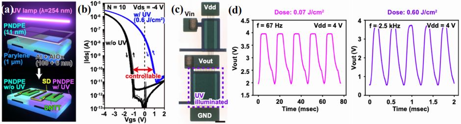
Vth of organic-TFT is controlled by photosensitive polymer gate insulator As concerns organic-TFT, the research group of Osaka University and AIST reported that Vth of organic-TFT could be controlled by making use of a photosensitive polymer gate insulator. Way to use double gate electrodes, way to adopt self-assembled monolayers (SAM) or O2 plasma, and way to modulate work function of gate electrode were reported as control method of Vth in the past. However, it's difficult for fine patterning by making use of their methods. Therefore, the research group tried to control Vth and enhance circuit characteristics by making use of a photosensitive polymer "PNDPE" as gate insulator. If UV light is irradiated to PNDPE, OH group is generated, as a result, Vth of organic-TFT is changed. In this experiment, an organic transistor with PNDPE gate insulator was produced on a parylene substrate. As figure 3-(a), Vth could be controlled by irradiance of UV light. Furthermore, an inverter circuit was produced (figure 3-(c)). Noise margin and frequency properties were enhanced by irradiating UV light to load transistor only.
Coating time of co-deposition and patterning is reduced by use of liquid crystalline organic semiconductor
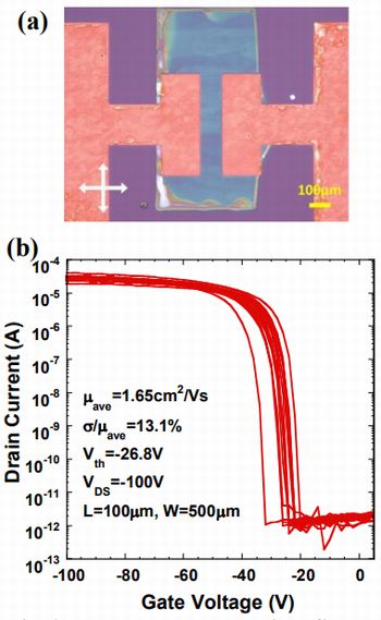
As you know, it's possible to pattern organic semiconductor film by coating technology at patterning-free using hydrophobic and hydrophilic treatment technology. The blade-coating method is widely used as its method. However, it's difficult to support uniform coating and speedy coating at the same time in above co-process. In fact, reported coating speed was mere a few �o/min. Therefore, the research group tried to coat at practical speed by use of liquid crystalline organic semiconductor, which is able to be highly oriented due to self-assembly. In experience, first of all, silicon substrate with thermal oxide SiO2 film was treated by hydrophobic and hydrophilic patterning technology. The next, dodecyltriethoxysilane was coated on whole of the substrate as hydrophobic SAM, and then, it in channel region only was eliminated, and phenyltriethoxysilane was coated as hydrophilic SAM. Subsequently, Au electrode was evaporated, and then, pentafluorothiophenol was coated on the electrode as SAM. Finally, liquid crystalline organic semiconductor liquid "Ph-BTBT-10" was coated at 900 mm/min by the blade-coating method. As a result, uniform and flat crystal could be coated at high speed, same as 100 times of that of the existing method. Carrier mobility and coefficient of variation of bottom gate/top contact device were 15.4 cm2/Vs and 18.8 % respectively. By the way, in this device, source/drain electrode was arranged in parallel with coating direction. For this reason, relatively high carrier mobility can be obtained by its structure. In fact, as figure 4-(a), grain boundary in crystal was not almost observed against coating direction because of growth of liquid crystal to coating direction. And also, figure 4-(b), in bottom gate/bottom contact device, which was a general structure for organic-TFT, average carrier mobility and coefficient of variation were 1.65 cm2/Vs and 13.1 % respectively. Light absorption layer of organic film solar cell is optimized by ESD with two supply sources As concerns organic series solar cell, Yamagata University reported a bulk-hetero junction organic film solar cell using electrostatic spray deposition (ESD) with two supply sources effectively.
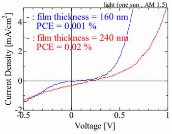
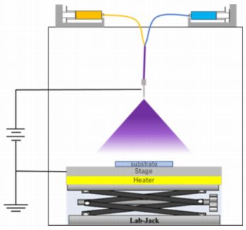
In this experiment, LiF film was evaporated on the substrate with ITO film as electron transport layer. The next, P3HT:PCBM active layer was deposited at 50 ��, 9V by ESD with two supply sources. In this time, under layer, upper layer, and middle layer became to be PCBM rich, P3HT-rich, and bulk-hetero junction respectively by optimization of liquid supply volume one another. By the way, CB and acetonitrile were used as a basic solvent and a solvent for spray. After deposition of active layer, its surface was planarized by SVA treatment (60 �� �~ 30 min) in CB environment. Finally, MoO3 film and Au were evaporated continuously as hole transport layer and upper electrode. Figure 6 shows J-V characteristics of samples. As a result, short-circuit current was increased in proportion as increase of film thickness. This is reason why generated exciton in balk-hetero layer is increased by increase of film thickness. In short, reduction of transport efficiency is decreased in case of thick film by making use of gradation in active layer, as a result, device property is enhanced. Reference 1)Yasuta, et.al.�FThermal stability of resistance of ion-implanted amorphous-InGaZnO film, The 68th JSAP Spring Meeting, 2021, 16-058 (2021.3) 2)Furuta, et.al.�FPolycrystalline IGO:H films for high-mobility thin-film transistors, The 68th JSAP Spring Meeting, 2021, 16-020 (2021.3) 3)Taguchi, et.al.�FPhotopatternable control of threshold voltage in flexible organic transistors, The 68th JSAP Spring Meeting, 2021, 11-357 (2021.3) 4)Kondo, et.al.�FFast speed fabrication of patterned organic semiconductor films by blade-coating using liquid crystalline organic semiconductor and their transistor characteristics, The 68th JSAP Spring Meeting, 2021, 11-353 (2021.3) 5)Ihashi, et.al.�FFabrication of inverted organic solar cells using electrostatic spray deposition with two supply sources, The 68th JSAP Spring Meeting, 2021, 11-094 (2021.3) |
| REMARK STELLA NEWS SITE is a free news site of FPD and PCB by Stella Corporation Inc.(This company does not release these FPD and PCB related products.) |
|