|
STELLA NEWS SITE is managed by Stella Corporation Inc. |

The 81th JSAP Autumn Meeting, 2020 (September 8 - 11) |
|||||||||||||||||||||||||||||||||||||||||||||||||||||||||||||||||||||||||||||||||||||||
September 8 - 11, The 81th JSAP Autumn Meeting, 2020 was held by online
method. Topics of OLED, organic-TFT, oxide-TFT, perovskite solar cell,
and manufacturing technology are closed up based on the proceeding.
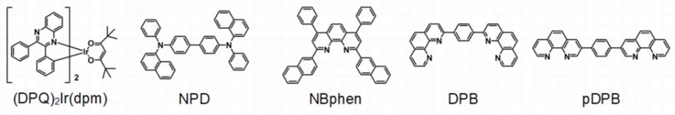
The next, a deep-red OLED was pilot-manufactured by using this co-evaporated emission layer. (DPQ)2Ir(dpm) with emission wavelength 670 nm was used as dopant material. This device is composed of ITO anode (130 nm)/polymer buffer layer (20 nm)/NPD hole transport layer (20 nm)/NPD:phenanthoroline derivative :(DPQ)2Ir(dpm)=50:50:1wt.% (40 nm) emitting layer/NBphen electron transport layer (50nm)/NBphen:20wt.%:Liq (20nm)/Liq buffer layer (1nm)/Al cathode (80nm).
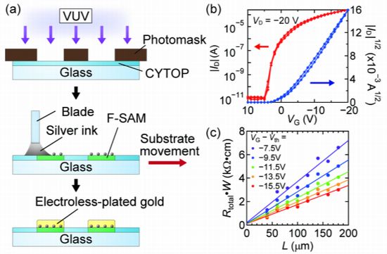
Soluble type electrode with high work function was formed damage-free against organic semiconductor With respect to organic-TFT, the research group of University of Tokyo, OPERANDO-OIL, JST and NIMS reported a new transfer process. In this process, an another substrate with formed metal electrode in advance by solution process is transferred to an original substrate with organic semiconductor layer due to damage-free against organic semiconductor.
Poly-para-xylene and soluble polymer (PVA) were coated on the substrate and dried, and then, the substrate was released. As a result, Au plated electrode film was completed. The next, p-type organic semiconductor C9-DNBDT-NW was stacked on monolayer crystal film, and then, PVA layer was dissolved in water. As a result, a source/drain electrode was transferred to the substrate. As figure 2-(b), high carrier mobility same as 13 cm2/V・s was obtained. And also, its contact resistance was relatively lower same as 120Ω・cm. In short, excellent carrier injection property was gained by this soluble electrode (figure 2-(c)). Anodically oxidized Al2O3 is effective for gate insulator of flexible IGZO-TFT As concerns oxide-TFT, Kochi University of Technology announced an IGZO (In-Ga-ZnO) -TFT with anodically oxidized Al2O3 gate insulator for flexible devices. As you know, the conventional SiOx gate insulator is not suitable for low thermal resistance substrate because of necessity of high temperature CVD deposition process (400 ℃ order). For this reason, anode oxidation was adopted in this time due to low temperature process.
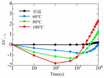
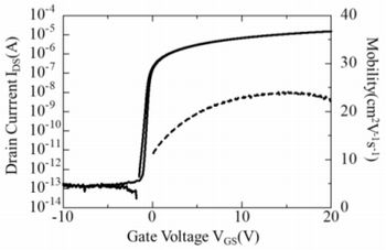
Figure 3 shows transfer characteristics of IGZO:H-TFT. Excellent properties were obtained, for example, carrier mobility = 24 cm2/V・s, Vth = -0.84V, S factor = 0.19 V/dec, and hysteresis = 0.22V. Figure 4 shows results of positive bias temperature stress test. It means change of Vth shift (ΔVth) at certain stress temperature (R.T.- 100 ℃) and applied voltage at +12 V for 104 seconds. In R.T.condition, ΔVth was greatly low same as 0.21 V after 104 seconds. By contrast, in high temperature conditions, Vth was shifted negatively until 103 seconds, on the other hand, was shifted positively since then. Furthermore, if stress temperature was increased, this trend became to be noticeable. Influence of solvent is researched in light absorption layer process of perovskite solar cell using 2 step method
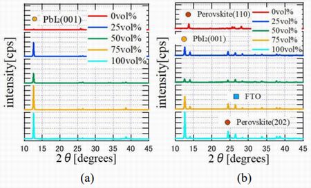
Deposition method of perovskite layer by solution process is classified into 1 step method using mixing liquid inclusive of all components and 2 step method, which is way to deposit PbI2 film and then treat by MAI. In the former, generation of crystal core and growth of crystal occur in the same time. On the other hand, in the latter, perovskite phenomenon is gradually generated, so that, perovskite grain is enlarged. In short, it's possible to gain excellent perovskite by using this 2 step method. In this research, influence of mixing solvent in precursor liquid using 2 step method was researched. As table 7 - (a), in case of using mixing solvent of DMSO and DMF, if ratio of DMSO solvent is increased, thickness of PbI2 film was decreased. And also, thickness of perovskite film itself was decreased because of dependence of PbI2 film. As table 7 - (a), if ratio of DMSO solvent is decreased, in spite of increase of thickness, peek strength of PbI2 (001) was decreased. This phenomenon means that amorphous area in the film was increased.
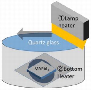
Grain size of perovskite is enlarged by zone-heating recrystallization Tokyo Institute of Technology proposed a new manufacturing process (zone-heating recrystallization method:ZHR method) of perovskite layer, in order to enlarge perovskite grain. This method has been proposed for silicon solar cell primitively. In this method, core growth area is controlled and surface flatness of silicon is enhanced by not only substrate anneal, but also lamp anneal. This technology was adopted for perovskite solar cell due to control of surface flatness and orientation.
As a result of observation by SEM, perovskite grain in all samples was enlarged, and its film thickness was kept. In fact, efficiency of all samples was enhanced. However, if treated time is long, device efficiency was decreased. It's reason why decomposition of perovskite is proceeded by uniform annealing of all surface of sample. In short, if the substrate is annealed at high temperature for relatively short time by ZHR method using lamp heating, device quality is enhanced because of enlargement of perovskite grain. Reference 1)Tsuneyama, et.al.:Stable deep-red phosphorescent OLEDs based on phenanthoroline-based n-type exciplex host, The 81th JSAP Autumn Meeting, 2020, 11-008 (2020.9) 2)Makita, et.al.:High-performance Organic Thin-film Transistors with Electroless-plated Gold Contacts, The 81th JSAP Autumn Meeting, 2020, 11-072 (2020.9) 3)Kouno, et.al.:Low-temperature processed In-Ga-Zn-O thin-film-transistors with an anodize Al2O3 gate insulator, The 81th JSAP Autumn Meeting, 2020, 16-009 (2020.9) 4)Ookawa, et.al.:Effect of mixture solvents for PbI2 film in perovskite layer fabricated using 2-step method, The 81th JSAP Autumn Meeting, 2020, 11-214 (2020.9) 5)Suzuki, et.al.:Relationship between enlarging grain size of perovskite layer and power generation property using zone-heating recrystallization method , The 81th JSAP Autumn Meeting, 2020, 11-215 (2020.9) |
|||||||||||||||||||||||||||||||||||||||||||||||||||||||||||||||||||||||||||||||||||||||
| REMARK STELLA NEWS SITE is a free news site of FPD and PCB by Stella Corporation Inc.(This company does not release these FPD and PCB related products.) |
|