|
STELLA NEWS SITE is managed by Stella Corporation Inc. |

The 79th JSAP Autumn Meeting, 2018 (September 18 - 21) |
||||||
September 18 - 21, The 79th JSAP Autumn Meeting, 2018 was held in Nagoya
International Congress Center. Topics of OLED, oxide-TFT, organic-TFT,
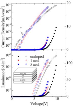
and CNT-TFT are closed up based on the proceeding. EIL and ETL of inverted OLED are optimized First, as regards OLED, Shinshu University reported that electron injection layer (EIL) and electron transporting layer (ETL) of inverted OLED were optimized.
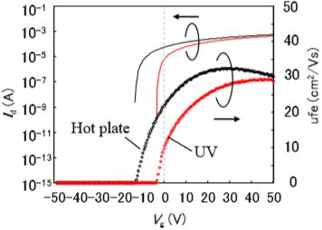
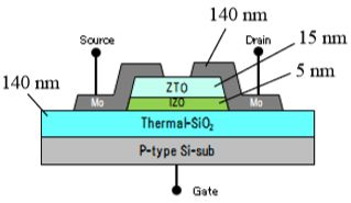
Figure 3 shows Id-Vg characteristics of TFTs. Vth of treated device by the atmosphere annealing was -13.5 V, on the other hand, that of treated device by UV annealing was -3.5 V. And also, in UV annealed device, high carrier mobility was obtained same as 29.5 cm2/V・s. In short, it's possible to not only lower process temperature, but also, to increase carrier mobility and to control Vth, too. ΔVth of organic-TFT is suppressed by use of hydrophobic gate dielectric About organic-TFT, the research group of University of Tokyo and National Institute of Advanced Industrial Science and Technology (AIST)announced characteristics of all solution process device with hydrophobic gate dielectric.
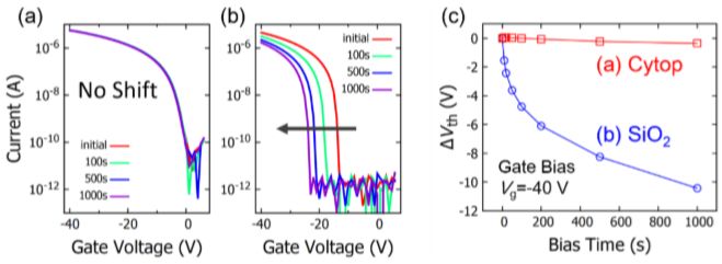
Figure 4 shows bias stress effects on transfer characteristics (Vd=−40 V) in N2 environment. As figure 4-(a), drain current of device with Cytop gate dielectric was decreased by mere 3 % and under. In short, bias stress stability was sufficient. On the other hand, as figure 4-(b), drain current of the reference device with SiOx gate dielectric and evaporated Au S/D electrodes was greatly decreased by 60 % and over due to occurrence of vth shift. Figure 4-(c) shows ΔVth of TFT with different gate dielectric. Vth shift of device with Cytop gate dielectric was greatly suppressed. Strain in channel region of CNT-TFT is locally suppressed for wearable device As concerns CNT-TFT, Nagoya University reported a CNT-TFT with stretchable characteristic for various wearable device.
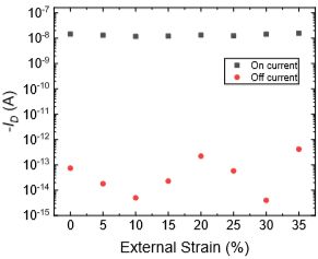
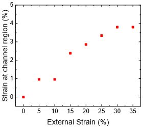
The device was turned at gate voltage = 5 V. Carrier mobility and ON/OFF current ratio were 7.2 cm2/V・s and 105 respectively. Figure 5 shows measured strain induced at channel region as a function of externally applied tensile strain. Strain at channel region was suppressed by 14 % of that of externally applied strain. Figure 6 shows ON and OFF currents as a function of externally applied tensile strain. If the device was stretched by 35 %, drain current was not changed. It suggested that local control of strain was effective. Reference 1)Taguchi, et.al.:Effects of Multi-layered Nano-hybrid Electron Buffer Layers for Improving the Blue Light Propaties of Inverted Polymer Light Emitting Diodes , The 79th JSAP Autumn Meeting, 2018, 11-238 (2018.9) 2)Moritsuka, et.al.:Evaluation of the high mobility Oxide TFTs by low temperature anneal, The 79th JSAP Autumn Meeting, 2018, 16-068 (2018.9) 3)Kitahara, et.al.:Stable Operation of Solution-Processed Organic Thin-Film Transistors Based on Ultrahydrophobic Carrier Transport Interface, The 79th JSAP Autumn Meeting, 2018, 11-215 (2018.9) 4)Nishio, et.al.:Low-voltage operable, stretchable carbon nanotube thin-film transistors with local strain control layer, The 79th JSAP Autumn Meeting, 2018, 15-160 (2018.9) |
| REMARK STELLA NEWS SITE is a free news site of FPD and PCB by Stella Corporation Inc.(This company does not release these FPD and PCB related products.) |
|