|
STELLA NEWS SITE is managed by Stella Corporation Inc. |

The 78th JSAP Autumn Meeting, 2017 (September 5-8,) |
||||||||
September 5-8, The 78th JSAP Autumn Meeting, 2017 was held in Fukuoka International Congress Center. Topics of OLED, organic-TFT, and manufacturing process technology were closed up based on the proceeding. Pt series green phosphorescence material with high color purity was reported
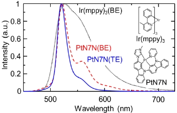
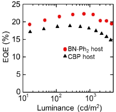
As concerns OLED, NHK reported extremely high color purity green phosphorescence material for wide color reproducibility of ultra-high resolution display such as 4K/8K TV. In this research, PtN7N (figure 2) was used as a green dopant. First of all, the research group measured PL spectrum of dispersed PtN7N in host material, to find out a suitable host material for this dopant. The conventional CBP, DIC-TRZ, and BN-Ph2 which were suitable for high efficiency respectively were used as a host material, as a result, full width at half maximum (FWHM) in DIC-TRZ was increased. For this reason, by use of CBP and BN-Ph2, which have narrow FWHM, bottom emission device were formed. As a result, FWHM of sample devices were greatly narrower than that of the reference device with Ir series complex dopant host, and then, extreme quantum efficiency of sample device was high same as maximum 22.2 % (figure 1, 2). Furthermore, a top emission device with micro cavity effect was manufactured, to be enhanced color purity. As a result, extremely high color purity same as x=0.18、y=0.74 was gained. This is reason why spectrum component of long wavelength range which was observed in the bottom emission device is expected to be suppressed. Light outcoupling efficiency of OLED is enhanced by low refractive index technology
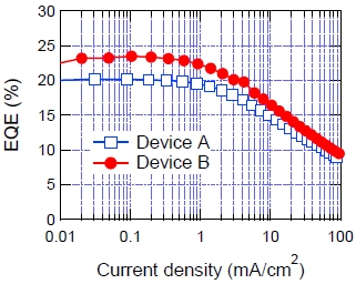
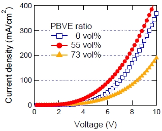
Yamagata University reported that light outcoupling efficiency of OLED was enhanced by use of organic thin film with low refractive index. In the past, the research group tried to lower refractive index by mixing fluorine series resin with organic semiconductor material. In this approach, conductive property was not almost changed; however, surface flatness of semiconductor layer was degraded and fluorine resin was decomposed. By contrast, in this time, flat ultra-low refractive index hole transport layer is formed successfully by making use of a new florin resin. In this experiment, perfluoro butenyl vinyl ether polymer (PBVE:refractive index 1.34@600nm) was mixed into the conventional HTL material α-NPD by co-evaporation method at 100 nm thickness. And also, the conventional phosphorescence device A (ITO/MoO3(5nm)/α-NPD(45nm)/8wt%-Ir(ppy)2(acac):CBP(15nm)/TPBi(65nm)/LiF(1nm)/Al) and new device B (ITO/MoO3(5nm)/55vol%-PBVE:α-NPD(60nm)/α-NPD(10nm)/8wt%-Ir(ppy)2(acac):CBP(15nm)/TPBi(60nm)/LiF(1nm)/Al) were manufactured respectively, and they were estimated.
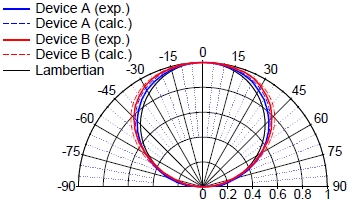
Figure 3 shows J-V characteristics of a hole only device (ITO/MoO3(5nm)/x vol%-PBVE:α-NPD(100nm)/MoO3(10nm)/Al). If PBVE was mixed at 55 vol%, conductive property of film was not changed, and then, refractive index of HTL was reduced to 1.54. Hole transport in mixed layer is accelerated by PBVE which has strong electron retention characteristic, as a result, decreased conductive property by mixing insulator material is sufficiently compensated. Figure 4 shows EQEs of the phosphorescent OLEDs with and without PBVE, figure 5 shows angular distributions of the emissions from the OLEDs. EQE of device A and B were 21.5 %, 25.9 % respectively. By contrast, light outcoupling efficiency of device A and B were 27.8 %, 33.3 % respectively. Considering PL quantum efficiency (83.6 %) of emitting layer, above EQE was confirmed to be almost repeated at actual measured value. In short, by mixing PBVE, refractive index of OLED was lowered and outcoupling efficiency was enhanced. All printable OTFT is manufactured by use of a new buffer layer For organic-TFT use, the research group of Yamagata University and Tosoh reported full printable device.
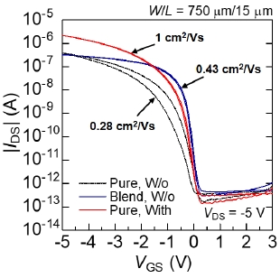
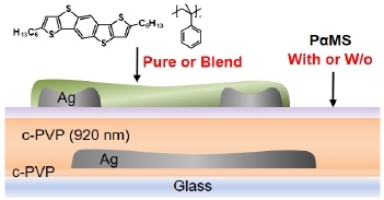
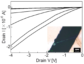
Figure 6 shows structure of the pilot-produced device, which is composed of the bottom-gate bottom-contact structure. All layers were formed by the printing process or the coating process. And also, annealing temperature was suppressed to 150 ℃ and under. Double layers of cross-liked PVP and PαMS buffer layer were used as a gate insulation layer. Source/drain and gate electrodes were formed by the IJ printing of Ag Nano size ink. And also, DTBDT-C6 ink or mixed ink of DTBDT-C6 and PαMS was printed as a semiconductor layer by the dispenser method. As figure 7, all devices operated at low voltage same as 5 V and under. Carrier mobility of device without buffer layer, device without buffer layer with mixed layer (DTBDT-C6 and PαMS), and device with buffer layer and DTBDT-C6 over layer were 0.28cm2/V・s, 0.43cm2/V・s, 1cm2/V・s respectively. And also, regarding various characteristics such as hysteresis, subthreshold slope, contact resistance, and so on, device with buffer layer showed most superior. This is reason why influence of carrier trap caused by adhered hydrogen molecule on surface of PVP insulation film and non-cross-liked and remained hydroxy group is reduced by forming of polymer buffer film. CNT film is directly patterned by the laser light focus As regards manufacturing process, Nikon proposed a new patterning method of CNT (Carbon Nano Tube). It's named as the laser direct drawing method.
In this experiment, first of all, CNT dispersed liquid is put on the glass substrate, and then, laser beam (975 nm) is irradiated at 100mW power from the reverse side of the substrate by use of a field lens. After laser incidence, CNT grains became deposited immediately from light focus point. CNT grains proceeded to deposit by scanning operation in the substrate, as a result, CNT pattern is gained by this direct patterning method. Spot size of light focus point was approximate 1 μm; on the other hand, that of CNT line width was 10 - 30 μm. However, fine line same as 1.5 μm was gained by optimization of process parameter, for example scanning speed, and etc. In this fact, CNT-TFT was manufactured by use of this CNT pattern as a channel, as a result, it showed as semiconductor property with relatively high carrier mobility same as 1.4 cm2/V・s. Reference |
| REMARK STELLA NEWS SITE is a free news site of FPD and PCB by Stella Corporation Inc.(This company does not release these FPD and PCB related products.) |
|