|
STELLA NEWS SITE is managed by Stella Corporation Inc. |

The 64th Japan Society of Applied Physics (JSAP) Spring Meeting 2017 (March 14-17) |
||||||||||||||||||||||||||||||||||||
March 14-17, “The 64th Japan Society of Applied Physics (JSAP) Spring Meeting 2017” was convened in Pacifico Yokohama. In this article, some notice oral lectures are picked up among OLED, Organic-TFT, oxide-TFT and process technology of electronics devices. TADF material for phosphorescence OLED is researched
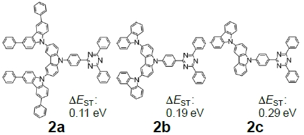
First of all, with respect to OLED, NHK reported the research result using TADF(Thermally Activated Delayed Fluorescence)as a host material of phosphorescence OLED. In this experiment, as figure 1, 3 kinds of materials (2a, 2b, 2c) were prepared as TADF emitting host. These materials have several carbazole groups as a donor and triazine groups as an acceptor, and also, have resident energy difference among singlet excited state and triplet excited state (ΔEST) respectively. By using these materials, test devices were pilot-produced. Its structure is composed of ITO anode/hole injection layer/α-NPD hole transporting layer/4DBTP3Q/host:Ir(mppy)/TPBi electron transporting layer/LiF buffer layer/Al cathode. Table 1 shows lifetime and external quantum efficiency (EQE) of test devices with these TDAF hosts, and EQE of test devices with these TADF dopants. Properties, especially, lifetime were depended on host materials in TADF host device. Concretely, good properties were gained in 2c device. On the other hand, in test device with TADF dopant, EQE of 2a device was best. In short, opposite movement against case of TADF host devices was observed. This means that if a TADF material is suitable for host, it concluded to be not exclusively suitable for phosphorescence dopant.
Furthermore, as table 1, 2c host device have longest lifetime because of small molecule and relatively large ΔEST. In short, TADF with small molecule is considered to be suitable lifetime of phosphorescence device. And also, device lifetime with TADF single film emitting layer was calculated, as a result, stability property of TADF material itself was almost same. For this reason, difference of lifetime is considered to be caused by difference of energy moving speed between host - dopant. High mobility IGZO-TFT is gained by ICP-sputtering
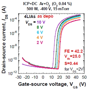
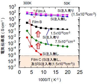
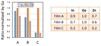
As regards oxide-TFT, the research group of Osaka University and EMD reported a-IGZO-TFT, which was deposited as oxide-semiconductor layer by plasma enhanced reactive sputtering deposition. In this deposition process, inductively coupled plasma (ICP)which is superimposed by magnetron discharge is controlled independently, in order to flow high density plasma in the vacuum chamber uniformly. Figure 2 shows electric characteristics of as-deposited device in 150 ℃. In this device, high carrier mobility same as 42.2 cm2/V・s was gained. This value is approximate 4 times of that of the conventional IGZO-TFT. And also, in post-annealing IGZO-TFT in 400 ℃, career mobility of O2 annealing device and N2 annealing device were 31.8cm2/V・s and 37.1cm2/V・s respectively. In short, if post-annealing process is introduced, higher mobility is gained compared to the conventional device. Reason of different mobility between N2 annealing device and O2 annealing device is considered that In:Ga:Zn composition of N2 annealing device (higher mobility) is changed from initial value (target composition) to In rich composition. Carrier density and bias stress stability are controlled by ion doping amount Tohoku University proposed that not only carrier density but also bias stress durability, which was a most problem for oxide-TFT were controlled by ion doping into a-IGZO film. In this experiment, first of all, a-IGZO film was deposited on the quartz substrate by the magnetron sputtering method. In this time, it was deposited by the co-sputtering using Ga2O3 target and IGZO target, so that, as figure 3, different samples such as Film A, Film B, and Film C were prepared by control of In:Ga:Zn ratio.
Subsequently, Si was doped into a-IGZO films. Dose amount is 5×1012cm-3 and 1×1013cm-3, doping density in the films is 7.5×1017cm-3 and 1.5×1018cm-3 respectively. The next, samples were annealed at 400 ℃ in wet environment (H2O/O2=100/900sccm) for 60 minutes. Figure 4 shows temperature dependence of electrical conductivity. While Si ion is doped into Film A, Film B, electrical conductivity is increased, especially, in Film B, electrical conductivity, in short, carrier density was found to be increased in proportion dose amount. On the other hand, in Film C which is rich Ga state, electrical conductivity was 10-5Scm-1 and under independently of with or without ion doping. Furthermore, bias stress durability was estimated by bias stress test (60 ℃, -30V×4000sec), as a result, in Film B device with doping 1.5×1018cm-3, Vth shift was confirmed to be greatly decreased. In short, ΔVth is expected to be controlled by Si dose amount. Fluorine doping is effective for wettable type IGZO-TFT, too
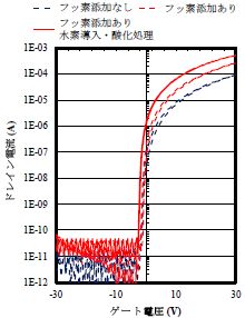
NHK reported estimate result of fluorine doping in wettable type IGZO-TFT. This treatment is considered to be effective for the sputtering deposition device. In this research, In(NO3)3・xH2O, Ga(NO3)3・xH2O, and Zn(CH3COO)c・2H2O, and fluorine additive agent (H2O+HF) were mixed and solved in pure water solvent, to prepare precursor liquid. This liquid was spin-coated on the silicon wafer with thermal oxide SiO2 film, and then, annealed at maximum 300 ℃. The next, this oxide-semiconductor film was patterned at island shape by the photolithography, and then, Mo source/drain electrode was deposited and patterned by mask-through evaporation method. Figure 5 Shows transfer characteristic of sample devices. Carrier mobility of device without fluorine doping was 1.8cm2/V・s, on the other hand, that of device with fluorine doping was 4.7 cm2/V・s. This is reason why trapping site such as oxygen defect was considered to be suppressed by fluorine doping. Moreover, S factor is enhanced from 0.48V/decade to 0.23V/dec. Furthermore, if hydrogen introduction and oxidation treatment process, which has been developed by this research group was added after deposition of IGZO film, high mobility such as 7 cm2/V・s at maximum was gained. This value is extremely high as wettable type IGZO-TFT. By the way, bias stress durability (+20V × 3000sec) is enhanced greatly, concretely, ΔVt was decreased from +3.1V to +0.6V. Organic semiconductor is orientated by laser irradiation With respect to organic-TFT, the research group of Kobe University and Nara Institute of Science and Technology reported that organic semiconductor was orientated by laser irradiation.
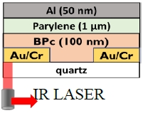
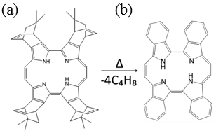
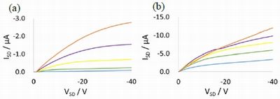
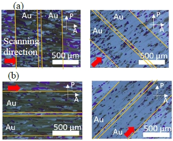
In this experiment, benzoporphycene (BPc) was used as organic semiconductor material. Its precursor material (BPc-Pre) was spin-coated on the quartz substrate with Au/Cr electrode (channel width=40 μm). The next, CO2 laser beam (10.6 μm) was irradiated against this substrate from back side vertically (BPc⊥) or parallel (BPc//), and swept as figure 7. Picture 1 shows polarized optical microscopy images after laser irradiation. If both films was rotated at an angle of 45°, light-dark was observed to reverse. And then, orientated Bpc crystal was formed between Au gap. Gate insulator film and Al gate electrode were formed on Bpc film; as a result, top gate-bottom contact TFT is manufactured. Figure 8 shows Vsd-Isd characteristic. Carrier mobility of Bpc⊥ device and BPc// device were 2.2×10⁻²cm2/V・s and 8.8×10⁻²cm2/V・s respectively. In short, that of BPc// device was approximate 4 times compared to that of Bpc⊥ device. This is reason why in BPc// device, grain boundaries in Au gap was decreased by forming of anisotropically large crystal against laser scanning direction.
Reference |
||||||||||||||||||||||||||||||||||||
| REMARK STELLA NEWS SITE is a free news site of FPD and PCB by Stella Corporation Inc.(This company does not release these FPD and PCB related products.) |
|