|
STELLA NEWS SITE is managed by Stella Corporation Inc. |

Shizuoka University New Technology Presentation Meetings (November 10th) |
|||
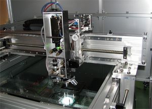
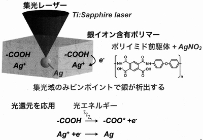
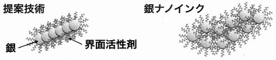
November 10th, “Shizuoka University New Technology Presentation Meetings” was held in JST (Tokyo). In this article, oral presentation of Atsushi Ono (associate professor)“Direct patterning technology of ultra-fine metal by irradiation of laser beam”is picked up. In this presentation, fine patterning process by use of laser beam was introduced;however, it is not same as mechanism of the conventional laser dry-etching process. As figure 1, Ag ion doped polymer such as polyimide precursor + AgNO3 is used as a substrate and conductive material. If laser beam is irradiated to the substrate, Ag is precipitated in irradiated area only selectively by photoreduction mechanism; as a result, Ag film is patterned with continuous state of Ag grains. In this process, it is possible to pattern at ultra-fine line such as laser wavelength and under by 2 photon photoreduction mechanism. In this experiment, ultra-fine line (minimum 200 nm) was patterned in spite of use of wavelength of 800 nm. Also, as figure 2, resistance of the film is expected to be lower than that of printed Ag Nano size ink or paste film, because influence of surfactant agent which covers with Ag grain, by continuous grain structure of Ag Nano size grains.
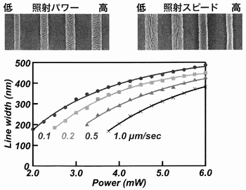
Figure 3 shows relationship of line width and irradiation power and speed. If irradiation power is high, line width becomes to be thick. On the other hand, irradiation speed is fast, it becomes to be fine. In short, line width can be controlled at will by these 2 process parameters. As you can image, main application is FPC with polyimide film. Furthermore, if Ag mesh wiring is added on polyimide film with ITO transparent electrode by making use of this process technology, it is easy to gain ultra-low resistance transparent electrode. Reference |
| REMARK STELLA NEWS SITE is a free news site of FPD and PCB by Stella Corporation Inc.(This company does not release these FPD and PCB related products.) |
|