|
STELLA NEWS SITE is managed by Stella Corporation Inc. |

The 63rd Japan Society of Applied Physics (JSAP) Spring Meeting 2016 (March 19-22) |
||||||||||||||||||
March 19-22, �gThe 63rd Japan Society of Applied Physics (JSAP) Spring Meeting 2016�h was convened in Tokyo Institute of Technology (Oookayama campus). In this article, some notice oral lectures are picked up among OLED, Organic-TFT, oxide-TFT and process technology of electronics devices. Lifetime is enhanced by use of new wettable HIL material
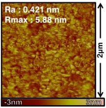
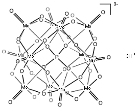
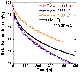
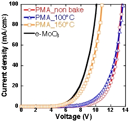
First of all, for OLED, research group of Yamagata University reported metal oxide HIL (Hole injection layer) material which is able to be deposited by various coating methods. In this experiment, phosphomolybdic and acid (PMA) with keggin structure (Fig.1) is used. It's inexpensive (about 100 yen/kg), dissolved in polar solvent, corresponded to low temperature process because of possibility of curing without burning, and transparent (90�� transmittance of invisible light). While acetonitrile liquid with this material was coated on the substrate, as picture 1, ultra-flat surface (Ra��0.421nm) was gained. Its value is superior to that of evaporated MoO3 film which is known as conventional metal oxide HIL material. For this reason, a sample device which was composed of ITO anode(130nm)/HIL(10nm)/��-NPD HTL(30nm)/CBP:Ir(ppy)3 EML(30nm)/BAlq3 HBL(10nm)/Alq3 HTL(40nm)/Liq buffer layer(1nm)/Al cathode(100nm) was manufactured, and its property was estimated. In this time, PMA device with baking process (100�� or 150��) at atmosphere and N2 environment, PMA device without baking process, and evaporated MoO3 device, and PEDOT/PSS device were prepared for comparison of device property.
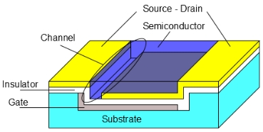
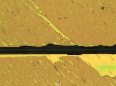
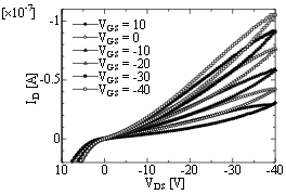
As a result, as figure 2, electric property of PMA device with baking process was almost same as that of e-MoO3 device. On the other hand, its lifetime property was superior to that of e-MoO3 device and PEDOT/PSS device. Wettable organic semiconductor film is deposited by making use of capillary phenomenon Research group of Chiba University announced a unique patterning process of wettable organic semiconductor for organic-TFT. Organic semiconductor material is filled into fine ditch by making use of capillary phenomenon. If this process is adopted, control of orientation is expected to be realized because of advantage of enhancement of device property. Research group estimated patterning characteristic of this process by making use of SVC-OFET which is their original device structure. Figure 4 shows structure of SVC-OFET. First of all, PET film substrate is fabricated by the nanoimprint method. As a result, fine ditch patterns (depth of 4.3 ��m, line width of 10 ��m) are formed on the substrate. The next, Al film is evaporated from oblique direction as gate electrode. Subsequently, parylen C is deposited vertically as gate insulator film. Furthermore, Au is evaporated obliquely from reverse direction against gate evaporation process as source/drain electrode. As a result, region without drain is generated on ditch because of shadow effect. This becomes to be channel of transistor. For this reason, fine channel such as sub ��m order can be formed easily. Finally, TIPS pentacene (concentration of 8mg/mL) is dropped on termination of ditch by use of syringe nozzle. As picture 2, TIPS pentacene proceeds into inside of ditch at self-aligning by capillary phenomenon and becomes to be filmed. Filling speed at depth of 2.25 ��m was 80 - 90 ��m/sec, and that at 4.3 ��m was 380 ��m/sec. In short, if aspect ratio is high, filling speed is up because of increase of capillary force. Also, in case of depth of 4.3 ��m, organic semiconductor material adhered to inside of ditch only; as a result, excellent patterning was realized. By contrast, in case of depth 2.25 ��m, it spread to surround, as a result, patterning characteristic was inefficient. Figure 5 shows output property of sample device. Its carrier mobility was 5.5�~10-4 cm2/V�s, ON/OFF current ratio was 23.9.
Dipping time of SAM is reduced greatly AIST reported that dipping time of SAM (Self Assembled Monolayers) was reduced greatly in manufacturing process of low voltage type organic transistor. In the past, research group has developed low voltage type organic transistor which was operated at mere 2 V. In this device, surface of Al gate is modified to AlOx film by O2 plasma treatment, and also, n-octadecylphosphonic acid is deposited on this gate as ultra-thin film gate insulator film. However, in the past reports inclusive of their experiment, SAM was deposited for long time such as 16 h by dipping process. Thus, in this time, they tried to reduce dipping time of SAM.
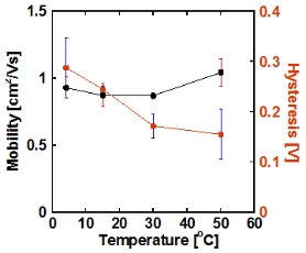
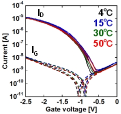
Process flow is as bellow�G�@Al gate is evaporated on the substrate, �AThe substrate is treated in vacuum environment by O2 plasma treatment, �BThe substrate is dipped into n-octadecylphosphonic acid, �CThe substrate is rinsed by use of isopropanol, �DThe substrate is annealed at 100 �� for 10 minutes. In manufactured DNTT device, while dipping time was 2 minutes and over, excellent carrier mobility was gained, for example, 1.1 cm2/V�s (for 2 minutes). This is reason why chemical reaction is completed for about 1 minute. On the other hand, if dipping time is long, Vth shift and hysteresis property are degraded. In short, best result is gained for 2 minutes. By contrast, if dipping time is long, morphology of film was not almost blowzy, and then, pure film is gained. On the other hand, if liquid temperature in dipping process is high, carrier mobility is increased. As figure 8, in case of dipping at 50 ��, hysteresis of device is decreased to 0.16 V which is half of that of dipping at 4 ��. This is reason why crystallization property and grain size of DNTT organic semiconductor is considered to be changed because of change of surface flatness by deposition state of SAM. Characteristics of solution-processed oxide-TFT is enhanced by hydrogen plasma treatment With respect to oxide-TFT, research group of NHK and AIST reported that characteristics of solution-processed oxide-TFT was enhanced by use of hydrogen plasma treatment, in order to remove impurity in oxide semiconductor film with keeping low temperature process (300 ��) for solution-processed oxide-TFT.
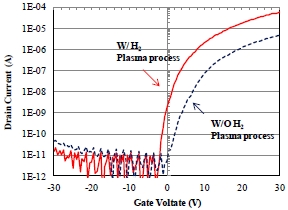
In this experiment, Zn-Tin-Oxide(ZTO) and In-Ga-Zn-O(IGZO) were prepared, and then, the former is dissolved into organic solvent, on the other hand, the latter is dissolved into water. These precursor liquids were spin-coated on the substrate, and then, annealed at 300 �� for 1 hour. The next, the substrate is treated by hydrogen plasma treatment at RF power of 100W and pressure of 8 Pa. Finally, it was annealed at 300 �� for 1 hour. It is reason why impurity is removed by reduction and resolution mechanism by hydrogen plasma treatment, on the other hand, oxidation is accelerated by post-anneal. In this estimation by TDS analysis, carbon and Cl were greatly decreased in the both TFTs. Carrier mobility of bottom-gate top-contact ZTO-TFT is enhanced from 1.8 cm2/V�s to 3 cm2/V�s by hydrogen plasma treatment. As figure 9, drain current is increased by hydrogen plasma treatment because of decrease of trap site by function of hydrogen, and also, oxidation was accelerated by post-anneal treatment. This is reason why oxidation is not accelerated insufficiently by low temperature anneal treatment (300 ��) in solution-processed oxide-TFT without their added treatments, as a result, organic substance remains into film as trap site. Inorganic EL is manufactured by use of IGZO emitting host Tokyo Institute of Technology which is a pioneer of oxide-TFT proposed to use a-IGZO for inorganic thin film EL as a new application. Research group verified that red inorganic EL could be manufactured easily by use of a-IGZO host and Eu guest. As you know, ZnS phosphor based inorganic EL has been developed in the past, and then, it is not novel. However, while this device is manufactured, it's necessary to anneal at high temperature such as 600 �� and over. For this reason, in this research, inorganic EL film was tried to be deposited at room temperature by making use of characteristic of a-IGZO. It's selected as emitting host material because of amorphous structure and low defect density.
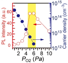
In this experiment, IGZO and Eu were co-deposited by the pulse laser deposition method using polycrystalline InGaZnO4 target. In this time, substrate temperature was controlled from room temperature to 500 ��. In any case, red emission (wavelength 614 nm) was observed because of derivation of Eu. Oxygen partial pressure (O2) is important for deposition process. As figure 10, it's necessary to deposit at 5 - 6 Pa. This value is double value of deposition of oxide semiconductor. This is reason why carrier density is lowered to 1013/cm3 order. By contrast, concentration of Eu is limited to maximum 30��. If concentration is 30 �� and over, concentration quenching occurs. Also, emission intensity showed best result in 400 �� deposition. It is double of case of room temperature deposition. On the other hand, in case of 500 �� deposition, emission intensity was decreased because of depletion of H2O in film. Reference |
||||||||||||||||||
| REMARK STELLA NEWS SITE is a free news site of FPD and PCB by Stella Corporation Inc.(This company does not release these FPD and PCB related products.) |
|